R01UH0823EJ0100 Rev.1.00 Page 533 of 1823
Jul 31, 2019
RX23W Group 23. Multi-Function Timer Pulse Unit 2 (MTU2a)
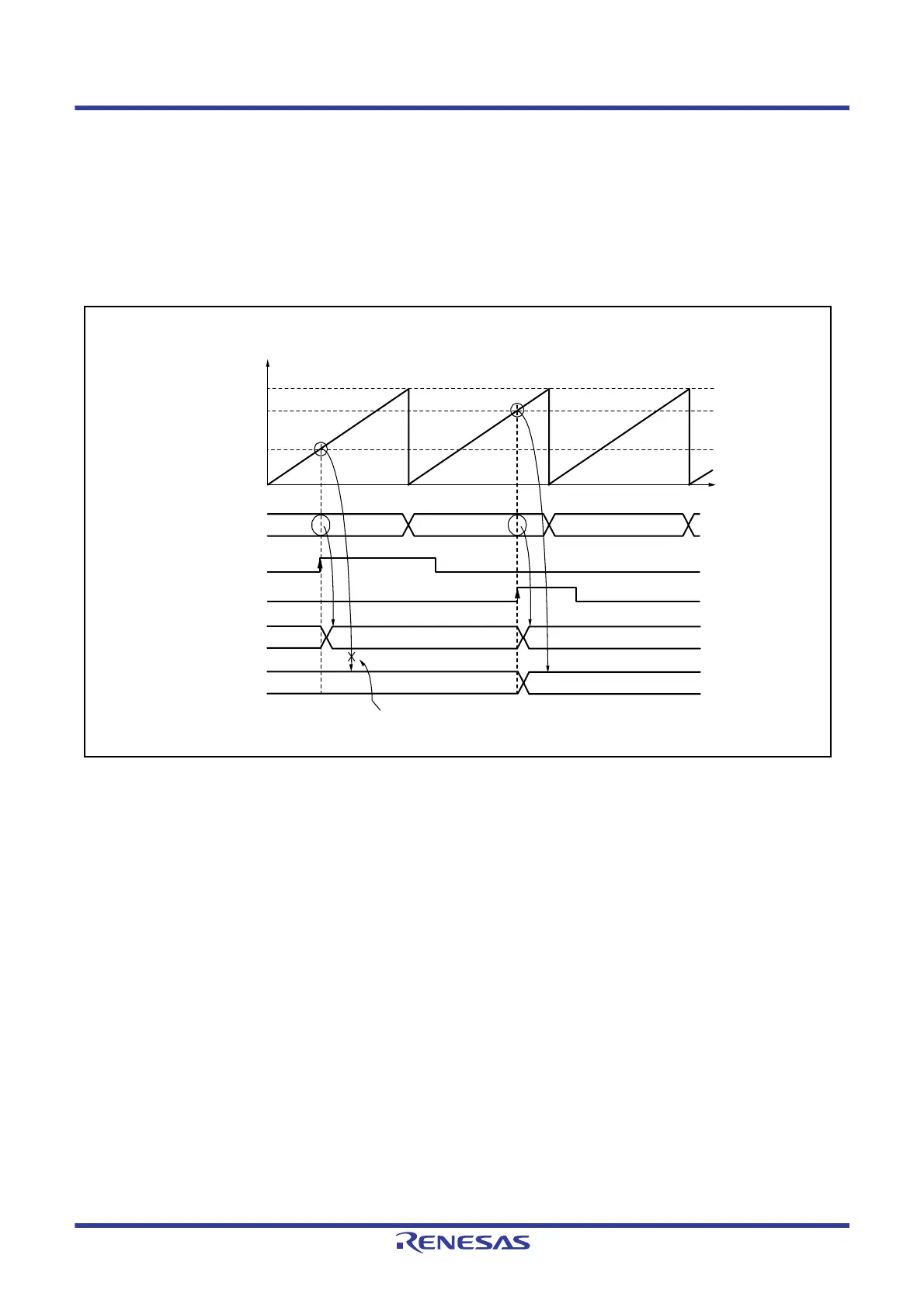
(3) Cascaded Operation Example (b)
Figure 23.22 illustrates the operation when counters MTU1.TCNT and MTU2.TCNT have been cascaded and the
TICCR.I2AE bit has been set to 1 to include the MTIOC2A pin in the MTU1.TGRA input capture conditions. In this
example, the MTU1.TIOR.IOA[3:0] bits have selected the MTIOC1A rising edge for the input capture timing while the
MTU2.TIOR.IOA[3:0] bits have selected the MTIOC2A rising edge for the input capture timing.
Under these conditions, the rising edge of both MTIOC1A and MTIOC2A is used for the MTU1.TGRA input capture
condition. For the MTU2.TGRA input capture condition, the MTIOC2A rising edge is used.
Figure 23.22 Cascaded Operation Example (b)
MTU2.TCNT value
Time
0514h0513h0512h
0513h0512h
C256h
As TICCR.I1AE is 0, data is not captured in MTU2.TGRA at
the MTIOC1A input timing.
0000h
MTU1.TGRA
MTU2.TGRA
MTIOC1A
MTIOC2A
MTU1.TCNT
C256h
FFFFh
6128h

 Loading...


