R01UH0823EJ0100 Rev.1.00 Page 577 of 1823
Jul 31, 2019
RX23W Group 23. Multi-Function Timer Pulse Unit 2 (MTU2a)
(c) Buffer Transfer Control Linked with Interrupt Skipping
In complementary PWM mode, whether to transfer data from a buffer register to a temporary register and whether to link
the transfer with interrupt skipping can be specified with the TBTER.BTE[1:0] bits.
Figure 23.70 shows an example of operation when buffer transfer is disabled (BTE[1:0] = 01b). While this setting is
valid, data is not transferred from the buffer register to the temporary register.
Figure 23.71 shows an example of operation when buffer transfer is linked with interrupt skipping (BTE[1:0] = 10b).
While this setting is valid, if data is written to the buffer register within the buffer transfer-enabled period, the data is
transferred immediately from the buffer register to the temporary register. If data is written to the buffer register outside
the buffer transfer-enabled period, the data is transferred from the buffer register to the temporary register at the timing
when the next buffer transfer-enabled period starts.
Note that the buffer transfer-enabled period depends on the TITCR.T3AEN bit and TITCR.T4VEN bit settings.
Figure
23.72
shows the relationship between the TITCR.T3AEN bit and TITCR.T4VEN bit settings and buffer transfer-
enabled period.
Note: This function must always be used in combination with interrupt skipping.
When interrupt skipping is disabled (the T3AEN and T4VEN bits in the TITCR register are set to 0 or the skipping
count setting bits (T3ACOR[2:0] and T4VCOR[2:0]) in the TITCR register are set to 000b), make sure that buffer
transfer is not linked with interrupt skipping (set the TBTER.BTE[1] bit to 0).
If buffer transfer is linked with interrupt skipping while interrupt skipping is disabled, buffer transfer is never
performed.
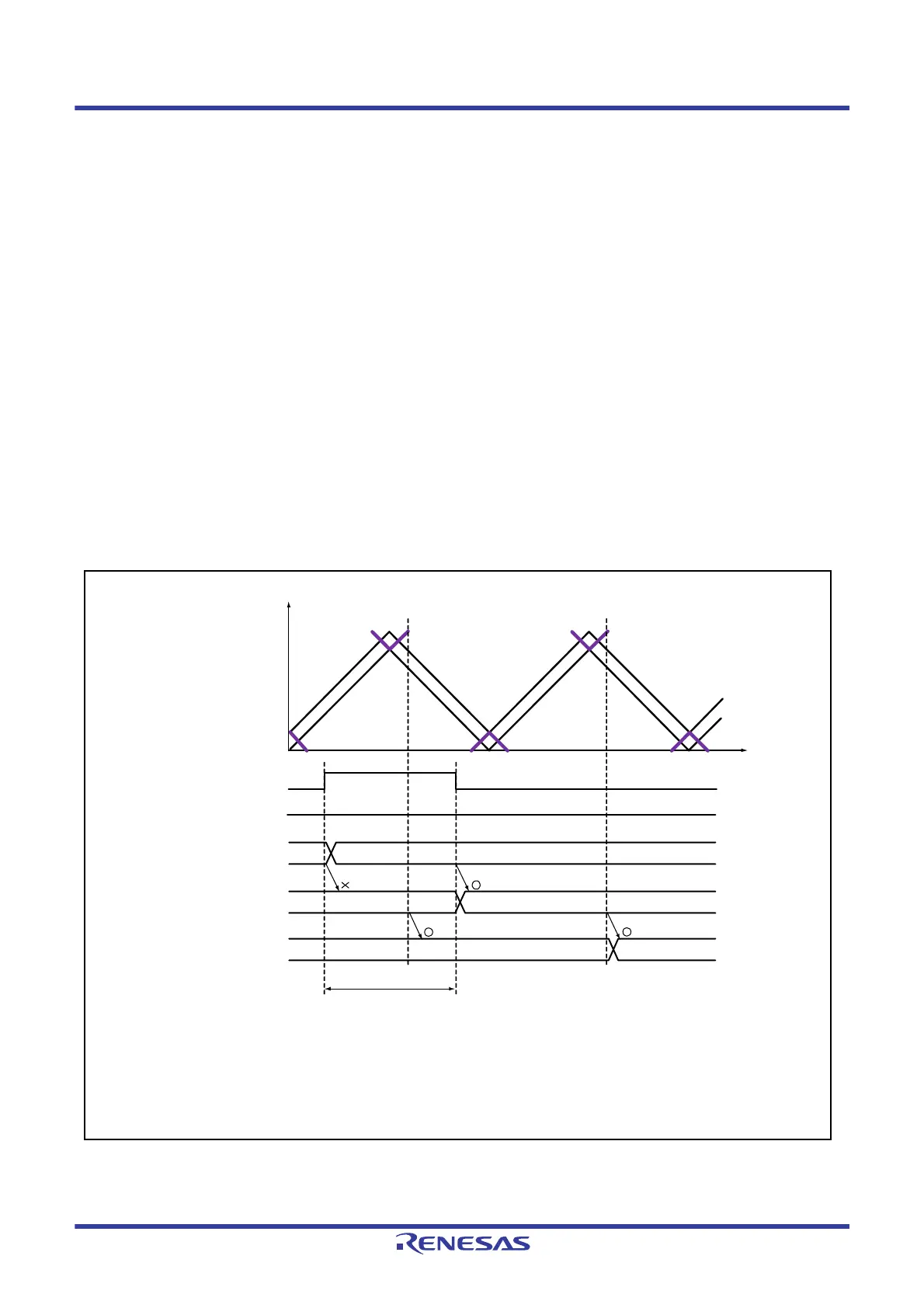
Figure 23.70 Example of Operation When Buffer Transfer is Disabled (TBTER.BTE[1:0] = 01b)
MTU3.
TCNT
MTU4.
TCNT
(1)
(2)
(3)
Buffer transfer is suppressed
Data 1
TBTER.BTE[1] bit
TBTER.BTE[0] bit
Temporary register
Buffer register
Compare register
Data 1 Data 2
Data 2
Data 2
Data
*
1
Data*
1
(1) No data is transferred from the buffer register to the temporary register in the buffer transfer-disabled period
(setting TBTER.BTE[1:0] to 01b).
(2) Data is transferred from the temporary register to the compare register even in the compare transfer-disabled
period.
(3) After buffer transfer is enabled, data is transferred from the buffer register to the temporary register.
Note 1. When buffer transfer at the crest is selected.

 Loading...


