R01UH0823EJ0100 Rev.1.00 Page 673 of 1823
Jul 31, 2019
RX23W Group 25. 16-Bit Timer Pulse Unit (TPUa)
x: Don’t care
Note 1. When the BFA bit in TPU3.TMDR is set to 1 (TPU3.TGRA and TPU3.TGRC are used for buffer operation) and TPU3.TGRC is
used as a buffer register, this setting is invalid and input capture/output compare is not generated.
Note 2. When the BFB bit in TPU3.TMDR is set to 1 (TPU3.TGRB and TPU3.TGRD are used for buffer operation) and TPU3.TGRD is
used as a buffer register, this setting is invalid and input capture/output compare is not generated.
Note 3. When the TPSC[2:0] bits in TPU4.TCR are set to 000b and PCLK/1 is used as the TPU3.TCNT count clock, this setting is invalid
and input capture is not generated.
Note 4. Selected by the ICSELD bit in TPU3.TMDR.
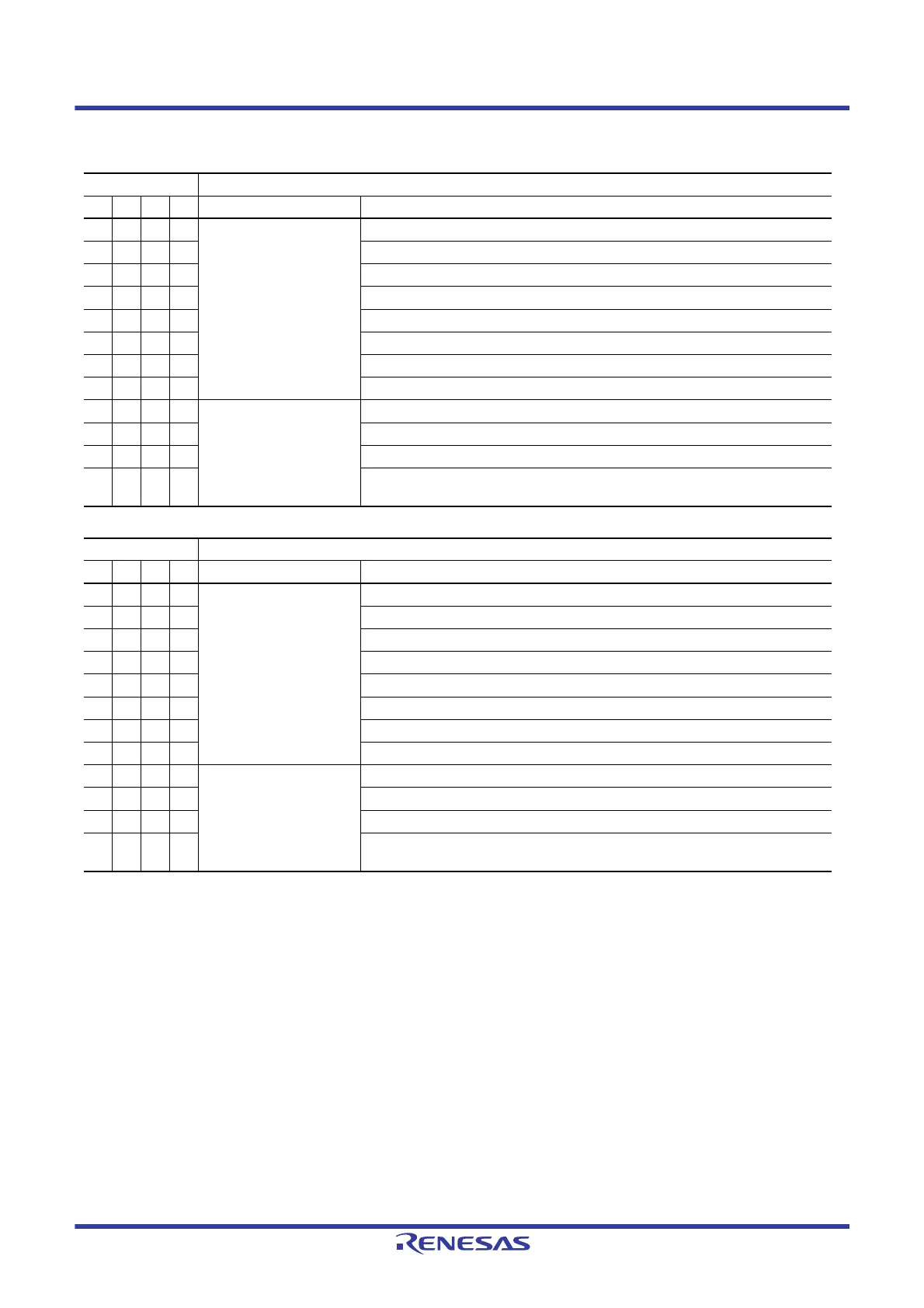
Table 25.19 TPU3.TIORL
Bits IOC[3:0] Description
b3 b2 b1 b0 TPU3.TGRC Function TIOCC3 Pin Function and Related Issue
0000Output compare register*
1
Output disabled
0001 Initial output is low output; low output at compare match
0010 Initial output is low output; high output at compare match
0011 Initial output is low output; toggle output at compare match
0100 Output disabled
0101 Initial output is high output; low output at compare match
0110 Initial output is high output; high output at compare match
0111 Initial output is high output; toggle output at compare match
1000Input capture register*
1
Capture input source is TIOCC3 pin; input capture at rising edge
1001 Capture input source is TIOCC3 pin; input capture at falling edge
1 0 1 x Capture input source is TIOCC3 pin; input capture at both edges
1 1 x x Capture input source is TPU4 count clock; input capture at TPU4.TCNT count-up/
count-down*
3
Bits IOD[3:0] Description
b7 b6 b5 b4 TPU3.TGRD Function TIOCD3 Pin Function and Related Issue
0000Output compare register*
2
Output disabled
0001 Initial output is low output; low output at compare match
0010 Initial output is low output; high output at compare match
0011 Initial output is low output; toggle output at compare match
0100 Output disabled
0101 Initial output is high output; low output at compare match
0110 Initial output is high output; high output at compare match
0111 Initial output is high output; toggle output at compare match
1000Input capture register*
2
Capture input source is TIOCD3 or TIOCC3 pin*
4
; input capture at rising edge
1001 Capture input source is TIOCD3 or TIOCC3 pin*
4
; input capture at falling edge
1 0 1 x Capture input source is TIOCD3 or TIOCC3 pin*
4
; input capture at both edges
1 1 X x Capture input source is TPU4 count clock; input capture at TPU4.TCNT count-up/
count-down*
3

 Loading...


