SPI_SCLK Edge Nr.
Sample
End
Begin
SPI_SCLK (POL = 0)
SPI_SCLK (POL = 1)
Data From the Master
Data From the Slave
Slave Select ( )
(optional)
SPI_SCS[n]
1 2
3
4
5
6
7
8 9 10
11 12
13
14
15 16
MSB
Bit6
Bit5
Bit4
Bit3
Bit2
Bit1
LSB
MSB
Bit6
Bit5
Bit4
Bit3
Bit2 Bit1
LSB
t
LEAD
t
LAG
Transfer
www.ti.com
Functional Description
269
SWRU543–January 2019
Submit Documentation Feedback
Copyright © 2019, Texas Instruments Incorporated
SPI (Serial Peripheral Interface)
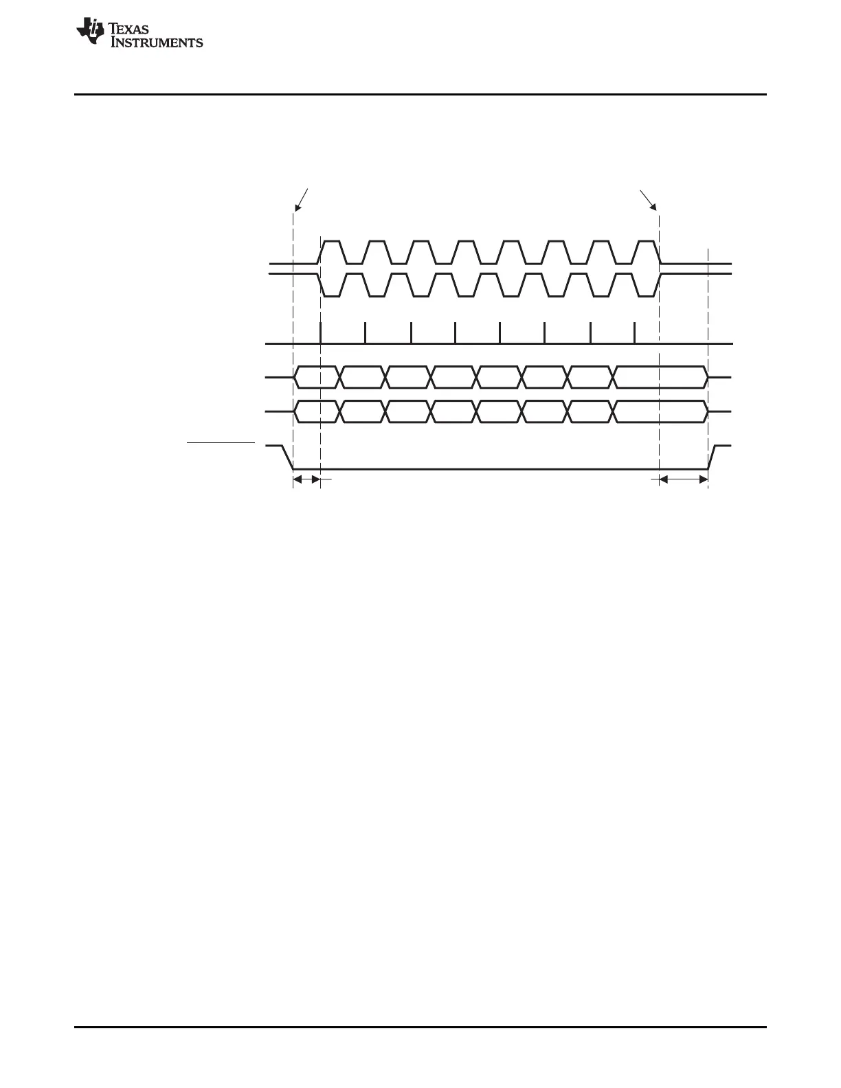
Figure 8-4 is a timing diagram of a SPI transfer for the SPI mode0 and SPI mode2, when the SPI is
master or slave, with the frequency of SPICLK equal to the frequency of CLKSPIREF.
Figure 8-4. Full-Duplex Single Transfer Format With PHA = 0
t
Lead
— Minimum leading time required for slave mode (ensured in master mode) before the first SPICLK
edge.
t
Lag
— Minimum trailing time required for slave mode (ensured in master mode) after the last SPICLK
edge.
In 3-pin mode without using the SPIEN signal, the controller provides the same waveform, with SPIEN
forced to low state. In 3-pin slave mode, SPIEN is useless.
8.2.2.2.5.2 Transfer Format With PHA = 1
This section describes SPI full-duplex transmission with the SPI mode1 and SPI mode3. In the transfer
format with PHA = 1, SPIEN is activated a delay (t
Lead
) ahead of the first SPICLK edge. In both master and
slave modes, the SPI drives the data lines on the first SPICLK edge.
Each data frame is transmitted starting with the MSB. At the extremity of both SPI data lines, the first bit of
the SPI word is valid on the next SPICLK edge, a half-cycle of SPICLK later, and is the sampling edge for
both the master and slave. When the third edge occurs, the received data bit is shifted into the shift
register. The next data bit of the master is provided to the serial input pin of the slave. This process
continues for a total number of pulses on the SPICLK line defined by the word length programmed in the
master device, with data being latched on even-numbered edges and shifted on odd-numbered edges.
Figure 8-5 is a timing diagram of a SPI transfer for the SPI mode1 and SPI mode3, when the SPI is
master or slave, with the frequency of SPICLK equal to the frequency of CLKSPIREF.





 To Next Page