After 8
Initial
Master SPI Shift
WordA
WordB
After 8
Initial
Slave SPI Shift Register
WordB
WordA
Shift Register
Transmitter Buffer
Control
Master
Receiver Register
Shift Register
Transmitter Buffer
Slave
Receiver Register
SPI_D[0] (MOSI)
SPI_D[1] (MISO)
SPI_SCLK
SPI_SCS[n]
(Optional)
Control
www.ti.com
Functional Description
267
SWRU543–January 2019
Submit Documentation Feedback
Copyright © 2019, Texas Instruments Incorporated
SPI (Serial Peripheral Interface)
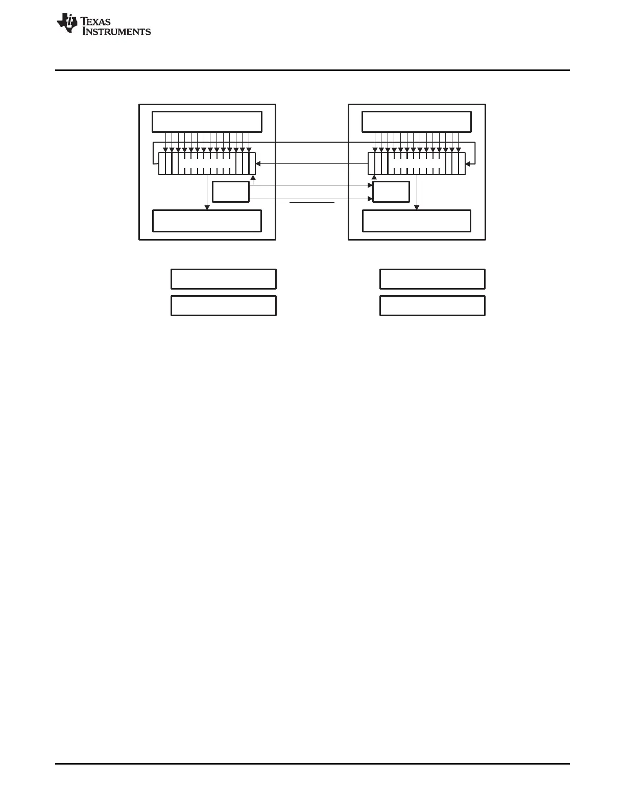
Figure 8-2. SPI Full-Duplex Transmission (Example)
When referring to the master device, the control block transmits the clock SPICLK and the enable signal
SPIEN.
8.2.2.2 Transfer Formats
This section describes the transfer formats supported by SPI. The flexibility of SPI allows setting the
parameters of the SPI transfer:
• SPI word length
• SPI enable generation programmable
• SPI enable assertion
• SPI enable polarity
• SPI clock frequency
• SPI clock phase
• SPI clock polarity
The software is responsible for the consistency between SPI word length, clock phase, and clock polarity
of the master SPI device and the communicating slave device.
8.2.2.2.1 Programmable Word Length
The SPI supports word lengths of 8, 16, and 32 bits.
8.2.2.2.2 Programmable SPI Enable (SPIEN)
The polarity of the SPIEN signals is programmable. SPIEN signals can be active high or low. The
assertion of the SPIEN signals is programmable: SPIEN signals can be manually asserted or
automatically asserted.
8.2.2.2.3 Programmable SPI Clock (SPICLK)
The phase and the polarity of the SPI serial clock are programmable when the SPI is a master device or a
slave device. The baud rate of the SPI serial clock is programmable when the SPI is a master. When the
SPI is operating as a slave, the serial clock SPICLK is an input from the external master.

 Loading...


