Register Description
www.ti.com
128
SWRU543–January 2019
Submit Documentation Feedback
Copyright © 2019, Texas Instruments Incorporated
Direct Memory Access (DMA)
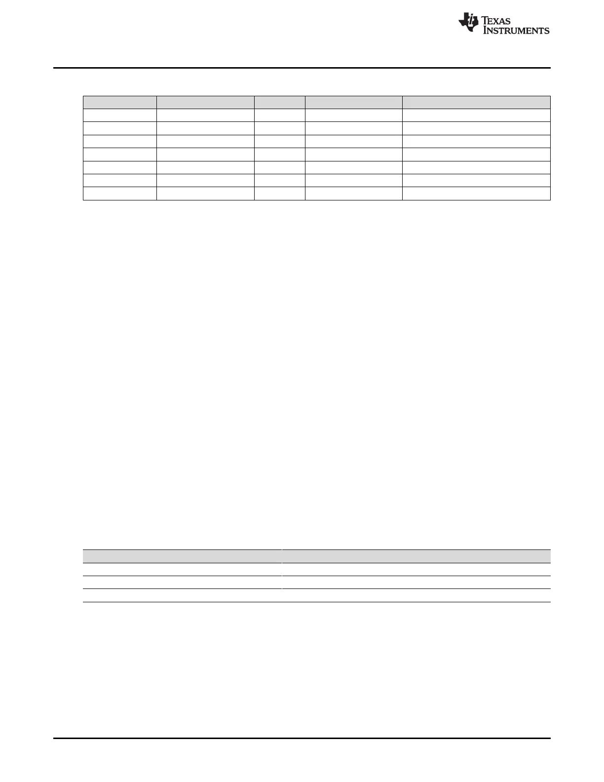
Table 4-5. µDMA Register Map (continued)
Offset Name Type Reset Description
0x04C DMA_ERRCLR R/W 0x0000.0000 DMA Bus Error Clear
0x500 DMA_CHASGN R/W 0x0000.0000 DMA Channel Assignment
0x510 DMA_CHMAP0 R/W 0x0000.0000 DMA Channel Map Select 0
0x514 DMA_CHMAP1 R/W 0x0000.0000 DMA Channel Map Select 1
0x518 DMA_CHMAP2 R/W 0x0000.0000 DMA Channel Map Select 2
0x51C DMA_CHMAP3 R/W 0x0000.0000 DMA Channel Map Select 3
0xFB0 DMA_PV RO 0x0000.0200 DMA Peripheral Version
4.3.2 µDMA Channel Control Structure
The µDMA channel control structure holds the transfer settings for a µDMA channel. Each channel has
two control structures, which are in a table in system memory. The channel control structure is one entry
in the channel control table. Each channel has a primary and alternate structure. The primary control
structures are at offsets 0x0, 0x10, 0x20 and so on. The alternate control structures are at offsets 0x200,
0x210, 0x220, and so on.
4.3.3 DMA Registers
Table 4-6 lists the memory-mapped registers for the
DMA_(OFFSET_FROM_CHANNEL_CONTROL_TABLE_BASE). All register offset addresses not listed in
Table 4-6 should be considered as reserved locations and the register contents should not be modified.
Table 4-6 lists the DMA channel control structures and registers. The channel control structure shows the
layout of one entry in the channel control table. The channel control table is in system memory, and the
location is determined by the application, thus the base address is N/A (not applicable) and is noted as
such above the register descriptions. In Table 4-6, the offset for the channel control structures is the offset
from the entry in the channel control table. See Channel Configuration table for description of how the
entries in the channel control table are in memory. The DMA register addresses are given as a
hexadecimal increment, relative to the DMA base address of 0x400F.F000.
The DMA module clock must be enabled before the registers can be programmed. There must be a delay
of three system clocks after the DMA module clock is enabled before any DMA module registers are
accessed. The DMA Channel Control Structure holds the transfer settings for a DMA channel. Each
channel has two control structures, which are in a table in system memory. The channel control structure
is one entry in the channel control table. Each channel has a primary and alternate structure. The primary
control structures are at offsets 0x0, 0x10, 0x20 and so on. The alternate control structures are at offsets
0x200, 0x210, 0x220, and so on.
Table 4-6. DM Registers
Offset Acronym Register Name Section
0h DMA_SRCENDP DMA Channel Source Address End Pointer Section 4.3.3.1
4h DMA_DSTENDP DMA Channel Destination Address End Pointer Section 4.3.3.2
8h DMA_CHCTL DMA Channel Control Word Section 4.3.3.3
 Loading...


