System
DMA
System
Interrupt
System
Clock
Unit
Local
Host
SPI Interface
Reference Clock
*CLK: Functional Reference Clock
DMA_TX_REQ[3:0]
WAKE_REQ
CLK*
SPI
(Master/Slave)
SPI_SCLK
SPI_D[0]
SPI_D[1]
(Touch Screen,
LCD, Audio
Codec, etc.)
External SPI Compliant Devices
(Single Master or Slave)
DMA_RX_REQ[3:0]
IRQ
www.ti.com
Overview
265
SWRU543–January 2019
Submit Documentation Feedback
Copyright © 2019, Texas Instruments Incorporated
SPI (Serial Peripheral Interface)
8.1 Overview
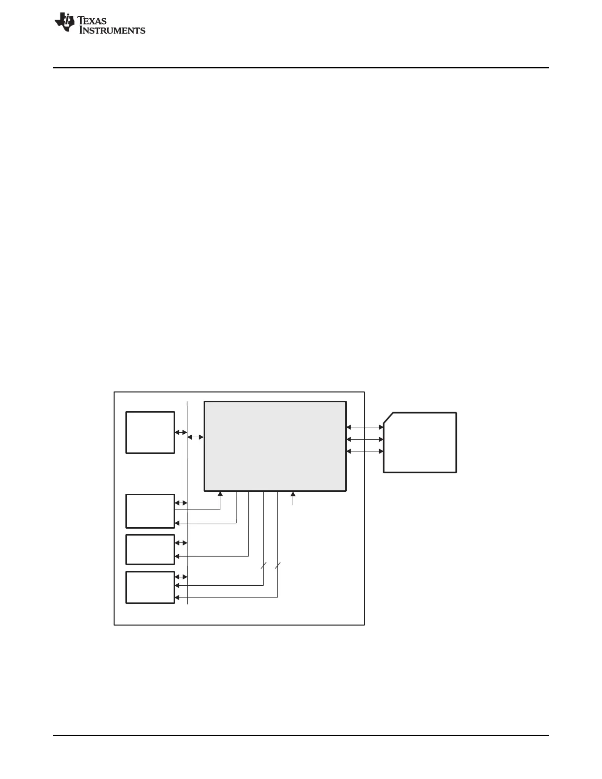
This chapter is intended to provide programmers with a functional presentation of the master and slave
serial peripheral interface module, and provides a module configuration example. The serial peripheral
interface (SPI) is a 4-wire bidirectional communications interface that converts data from parallel to serial.
The CC32xx device has two SPI interfaces:
• One SPI (master) interface is reserved for interfacing an external serial flash to the CC32xx. The serial
flash holds the application image and networking credentials, policies, and software patches. This is
referred to as the FLASH_SSPI; it has a fixed mapping to package pins.
• The second SPI can be used by the application in either master or slave mode. Refer to Section 8.6 for
the supported pin mapping options for this interface and the state of the pins in various sleep and reset
states. CLKSPIREF is the clock input to the SPI module, and has a gating in the PRCM module (refer
to on clock-reset-power management). The subdivision of this clock is inside the SPI module. The
CC32xx does not support waking up the chip on SPI activity.
This chapter focuses on the second SPI.
The SPI module performs serial-to-parallel conversion on data received from a peripheral device, and
parallel-to-serial conversion on data transmitted to a peripheral device. The SPI module can be configured
as either a master or slave device. As a slave device, the SPI module can also be configured to disable its
output, which allows a master device to be coupled with multiple slave devices. The TX and RX paths are
buffered with separate internal FIFOs. The SPI module also includes a programmable bit rate clock divider
to generate the output serial clock derived from the input clock of the SPI module. Bit rates are generated
based on the input clock, and the maximum bit rate is determined by the connected peripheral.
The SPI allows full duplex between a local host and SPI-compliant external devices (slaves and masters).
Figure 8-1 shows a high-level overview of the SPI system.
Figure 8-1. SPI Block Diagram
8.1.1 Features
• Serial clock with programmable frequency, polarity, and phase
• SPI enable
– Generation programmable
– Programmable polarity
• Selection of SPI word lengths at 8, 16, and 32 bits