Flash Registers
www.ti.com
776
SWRU543–January 2019
Submit Documentation Feedback
Copyright © 2019, Texas Instruments Incorporated
On-Chip Parallel Flash
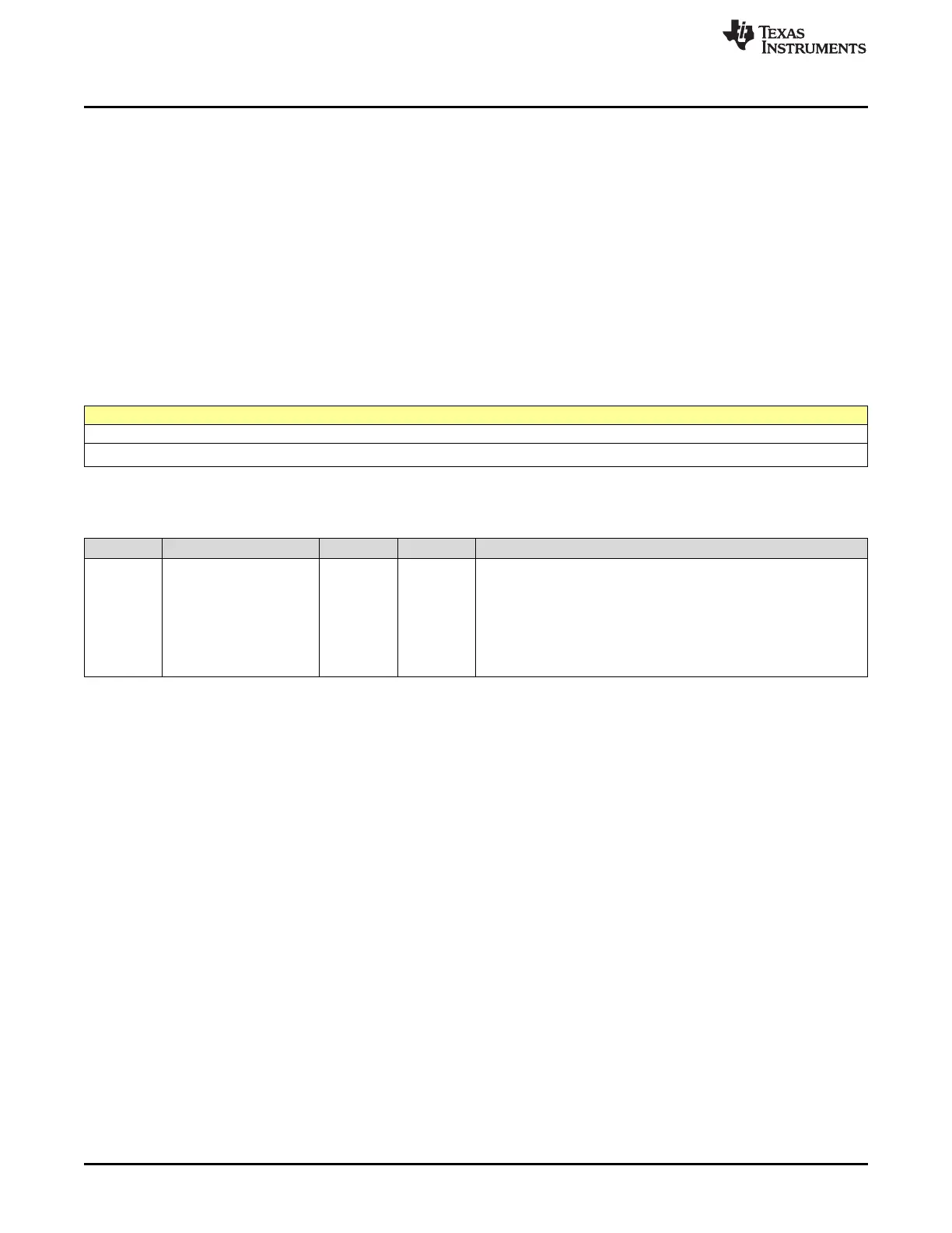
21.5.8 FWBVAL Register (Offset = 30h) [reset = 0h]
FWBVAL is shown in Figure 21-8 and described in Table 21-9.
Return to Summary Table.
This register provides a bitwise status of which FWBn registers have been written by the processor since
the last write of the flash memory write buffer. The entries with a 1 are written in the next write of the flash
memory write buffer.
This register is cleared after the write operation by hardware. A protection violation on the write operation
also clears this status.
Software can program the same 32 words to various flash memory locations by setting the FWB[n] bits
after they are cleared by the write operation. The next write operation then uses the same data as the
previous one. In addition, if an FWBn register change should not be written to flash memory, software can
clear the corresponding FWB[n] bit to preserve the existing data when the next write operation occurs.
Figure 21-8. FWBVAL Register
31 30 29 28 27 26 25 24 23 22 21 20 19 18 17 16 15 14 13 12 11 10 9 8 7 6 5 4 3 2 1 0
FWB[n]
R/W-0h
LEGEND: R/W = Read/Write; R = Read only; W1toCl = Write 1 to clear bit; -n = value after reset
Table 21-9. FWBVAL Register Field Descriptions
Bit Field Type Reset Description
31-0 FWB[n] R/W 0h
Flash Memory Write Buffer
Bit 0 corresponds to FWB0, offset 0x100, and bit 31 corresponds to
FWB31, offset 0x13C.
0h = The corresponding FWBn register has no new data to be
written.
1h = The corresponding FWBn register has been updated since the
last buffer write operation and is ready to be written to flash memory.

 Loading...


