Functional Description
www.ti.com
208
SWRU543–January 2019
Submit Documentation Feedback
Copyright © 2019, Texas Instruments Incorporated
Inter-Integrated Circuit (I
2
C) Interface
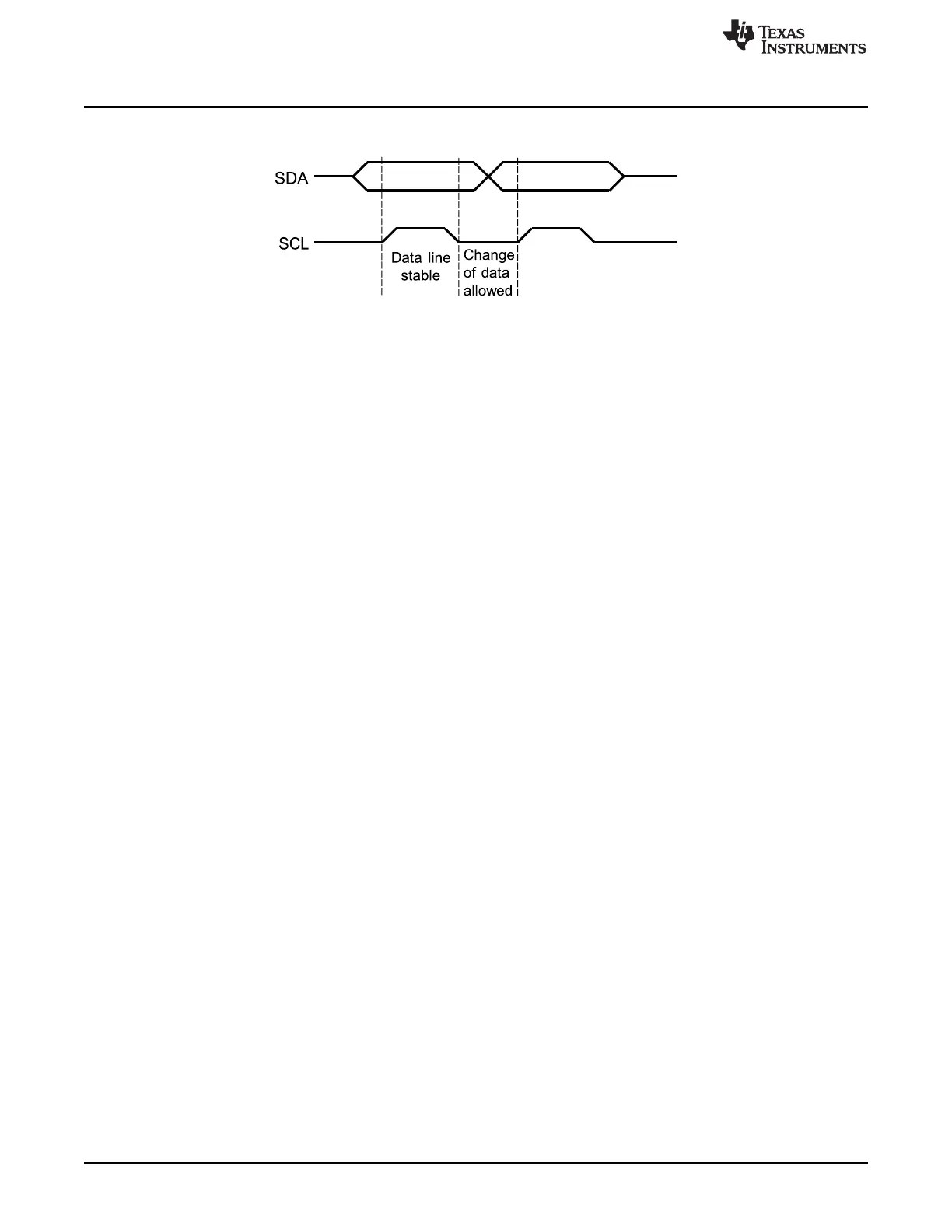
Figure 7-6. Data Validity During Bit Transfer on the I2C Bus
7.2.1.4 Acknowledge
All bus transactions have a required acknowledge clock cycle generated by the master. During the
acknowledge cycle, the transmitter (which can be the master or slave) releases the SDA line. To
acknowledge the transaction, the receiver must pull down SDA during the acknowledge clock cycle. The
data transmitted out by the receiver during the acknowledge cycle must comply with the data validity
requirements described in Section 7.2.1.3.
When a slave receiver does not acknowledge the slave address, SDA must be left high by the slave so
that the master can generate a STOP condition and abort the current transfer. If the master device acts as
a receiver during a transfer, it is responsible for acknowledging each transfer made by the slave. Because
the master controls the number of bytes in the transfer, it signals the end of data to the slave transmitter
by not generating an acknowledge on the last data byte. The slave transmitter must then release SDA to
allow the master to generate the STOP or a repeated START condition.
If the slave is required to provide a manual ACK or NACK, the I2C Slave ACK Control (I2CSACKCTL)
register allows the slave to NACK for invalid data or command or ACK for valid data or command. When
this operation is enabled, the MCU slave module I2C clock is pulled low after the last data bit, until this
register is written with the indicated response.
7.2.1.5 Repeated Start
The I2C master module has the capability of executing a repeated START (transmit or receive) after an
initial transfer has occurred.
A repeated start sequence for a master transmit is as follows:
1. When the device is in the IDLE state, the master writes the slave address to the I2CMSA register and
configures the R/S bit for the desired transfer type.
2. Data are written to the I2CMDR register.
3. When the BUSY bit in the I2CMCS register is 0, the master writes 0x3 to the I2CMCS register to
initiate a transfer.
4. The master does not generate a STOP condition, but instead writes another slave address to the
I2CMSA register, then writes 0x3 to initiate the repeated START.
A repeated start sequence for a master receive is similar:
1. When the device is in IDLE state, the master writes the slave address to the I2CMSA register and
configures the R/S bit for the desired transfer type.
2. The master reads data from the I2CMDR register.
3. When the BUSY bit in the I2CMCS register is 0, the master writes 0x3 to the I2CMCS register to
initiate a transfer.
4. The master does not generate a STOP condition, but instead writes another slave address to the
I2CMSA register, then writes 0x3 to initiate the repeated START.

 Loading...


