www.ti.com
UART Registers
181
SWRU543–January 2019
Submit Documentation Feedback
Copyright © 2019, Texas Instruments Incorporated
Universal Asynchronous Receivers/Transmitters (UARTs)
6.3 UART Registers
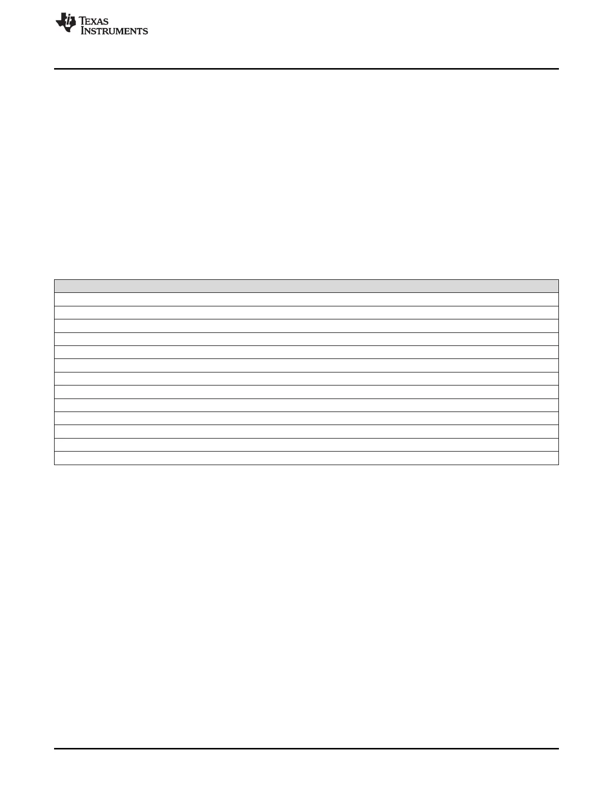
Table 6-2 lists the memory-mapped registers for the UART. All register offset addresses not listed in
Table 6-2 should be considered as reserved locations and the register contents should not be modified.
The offset listed is a hexadecimal increment to the register’s address, relative to that UART’s base
address:
• UART0: 0x4000.C000
• UART1: 0x4000.D000
The UART module clock must be enabled before the registers can be programmed. There must be a
delay of 3 system clocks after the UART module clock is enabled before any UART module registers are
accessed.
The UART must be disabled (see the UARTEN bit in the UARTCTL register) before any of the control
registers are reprogrammed. When the UART is disabled during a TX or RX operation, the current
transaction is completed prior to the UART stopping.
Table 6-2. UART Registers
Offset Acronym Register Name Section
0h UARTDR UART Data Section 6.3.1
4h UARTRSR_UARTECR UART Receive Status/Error Clear Section 6.3.2
18h UARTFR UART Flag Section 6.3.3
24h UARTIBRD UART Integer Baud-Rate Divisor Section 6.3.4
28h UARTFBRD UART Fractional Baud-Rate Divisor Section 6.3.5
2Ch UARTLCRH UART Line Control Section 6.3.6
30h UARTCTL UART Control Section 6.3.7
34h UARTIFLS UART Interrupt FIFO Level Select Section 6.3.8
38h UARTIM UART Interrupt Mask Section 6.3.9
3Ch UARTRIS UART Raw Interrupt Status Section 6.3.10
40h UARTMIS UART Masked Interrupt Status Section 6.3.11
44h UARTICR UART Interrupt Clear Section 6.3.12
48h UARTDMACTL UART DMA Control Section 6.3.13