www.ti.com
Pin Mapping Recommendations
607
SWRU543–January 2019
Submit Documentation Feedback
Copyright © 2019, Texas Instruments Incorporated
I/O Pads and Pin Multiplexing
(1)
Pins marked (wake) can be configured to wake up the chip from hibernate or LPDS state. In the current silicon revision, any wake pin can trigger wake up from hibernate. The wake-up
monitor in the hibernate control module logically ORs these pins applying a selection mask. However, wakeup from LPDS state can be triggered only by one of the wake-up pins that can
be configured before entering LPDS. The core digital wake-up monitor uses a mux to select one of these pins to monitor.
(2)
The device supports the feeding of an external 32.768-kHz clock. This configuration frees one pin (32K_XTAL_N) to use in output-only mode with a 100K pullup.
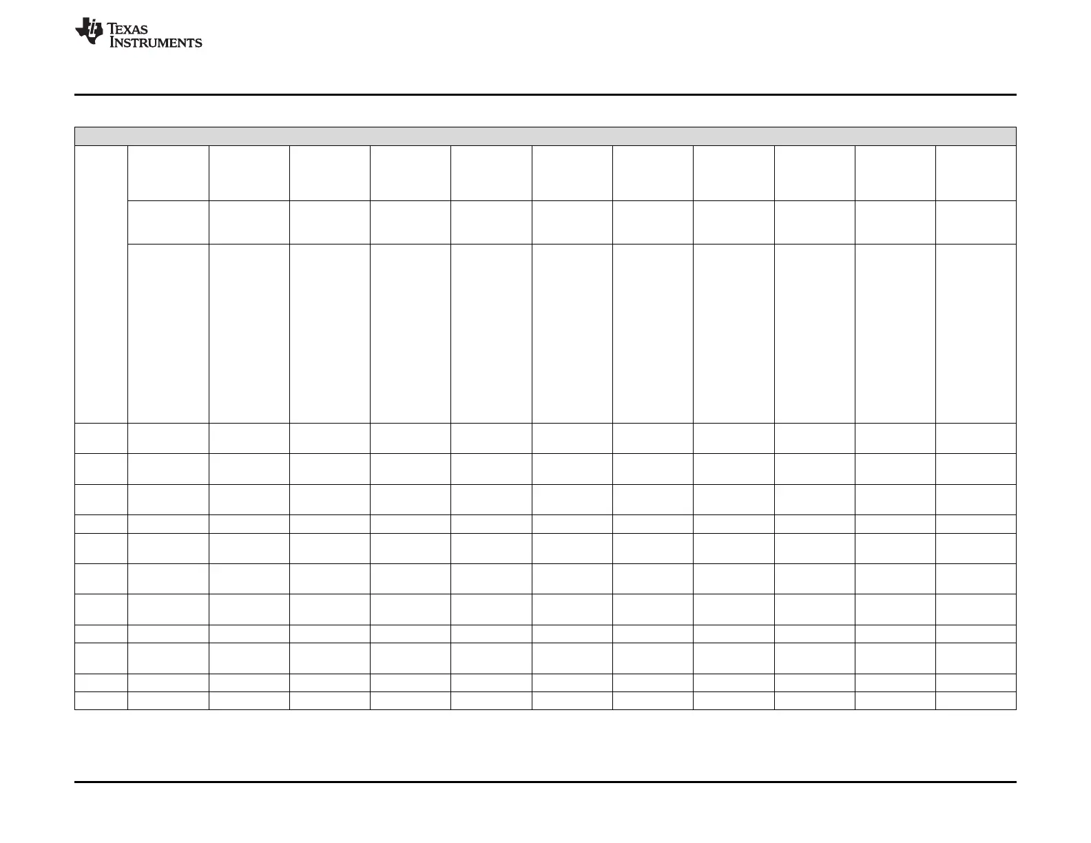
Table 16-13. Recommended Pin Multiplexing Configurations
CC32xx Recommended Pinout Grouping Use – Examples
(1)
Home
Security High-
end Toys
Wi-Fi Audio
++ Industrial
Sensor-Tag Home
Security Toys
Wi-Fi Audio
++ Industrial
Wi-Fi Remote
w/ 7 × 7
keypad and
audio
Sensor Door-
Lock Fire-
Alarm Toys
Without Cam
Industrial
Home
Appliances
Industrial
Home
Appliances
Smart-Plug
Industrial
Home
Appliances
GPIOs
External
32 kHz
(2)
External
32 kHz
(2)
External
TCXO 40 MHz
(-40 to +85°C)
Cam + I2S (Tx
or Rx) + I2C +
SPI + SWD +
UART-Tx +
(App Logger)
2 GPIO +
1PWM + *4
overlaid
wakeup from
Hib
I2S (Tx and
Rx) + 1 Ch
ADC + 1x
4wire UART +
1x 2wire
UART + 1bit
SD Card +
SPI + I2C +
SWD + 3
GPIO + 1
PWM + 1
GPIO with
Wake-From-
Hib
I2S (Tx and
Rx) + 2 Ch
ADC + 2wire
UART + SPI +
I2C + SWD +
2 PMW + 6
GPIO + 3
GPIO with
Wake-From-
Hib
Cam + I2S (Tx
or Rx) + I2C +
SWD + UART-
Tx + (App
Logger) 4
GPIO +
1PWM + *4
overlaid
wakeup from
HIB
I2S (Tx and
Rx) + 1 Ch
ADC + 2x
2wire UART +
1bit SD Card
+ SPI + I2C +
SWD + 4
GPIO + 1
PWM + 1
GPIO with
Wake-From-
Hib
I2S (Tx and
Rx) + 1 Ch
ADC + UART
(Tx Only) I2C
+ SWD + 15
GPIO + 1
PWM + 1
GPIO with
Wake-From-
Hib
I2S (Tx or Rx)
+ 2 Ch ADC +
2 wire UART
+ SPI + I2C +
3 PMW + 3
GPIO with
Wake-From-
Hib + 5 GPIO
SWD +
4 Ch ADC +
1x 4wire
UART + 1x
2wire UART +
SPI + I2C +
SWD + 1
PWM + 6
GPIO + 1
GPIO with
Wake-From-
Hib Enable for
Ext 40 MHz
TCXO
3 Ch ADC +
2wire UART +
SPI + I2C +
SWD + 3
PWM + 9
GPIO + 2
GPIO with
Wake-From-
Hib
2 Ch ADC +
2wire UART +
I2C + SWD +
3 PWM + 11
GPIO + 5
GPIO with
Wake-From-
Hib
Pin
Number
Pinout 11 Pinout 10 Pinout 9 Pinout 8 Pinout 7 Pinout 6 Pinout 5 Pinout 4 Pinout 3 Pinout 2 Pinout 1
52 GSPI-MOSI McASP-D0
(Tx)
GPIO_32
output only
53 GSPI-MISO MCASP-
ACLKX
MCASP-
ACLKX
GPIO_30 GPIO_30 GPIO_30 GPIO_30 UART0-TX GPIO_30 UART0-TX GPIO_30
45 GSPI-CLK McASP-AFSX McASP-D0 GPIO_31 McASP-AFSX McASP-AFSX McASP-AFSX UART0-RX GPIO_31 UART0-RX GPIO_31
50 GSPI-CS McASP-D1
(Rx)
McASP-D1 McASP-D1 McASP-D1 McASP-D1 McASP-D1 UART0-CTS GPIO_0 GPIO_0 GPIO_0
55 pCLK
(PIXCLK)
UART0-TX UART0-TX PIXCLK UART0-TX UART0-TX UART0-TX GPIO-1 UART0-TX GPIO_1 GPIO_1
57 (wake) GPIO2 UART0-RX UART0-RX (wake) GPIO2 UART0-RX GPIO_2 UART0-RX ADC-0 UART0-RX (wake)
GPIO_2
(wake)
GPIO_2
58 pDATA7 (D3) UART1-TX ADC-CH1 pDATA7 (D3) UART1-TX GPIO_3 ADC-1 ADC-1 ADC-1 ADC-1 GPIO_3
59 pDATA6 (D2) UART1-RX (wake)
GPIO_4
pDATA6 (D2) UART1-RX GPIO_4 (wake)
GPIO_4
ADC-2 ADC-2 (wake)
GPIO_4
(wake)
GPIO_4
60 pDATA5 (D1) ADC-3 ADC-3 pDATA5 (D1) ADC-3 ADC-3 ADC-3 ADC-3 ADC-3 ADC-3 GPIO_5
61 pDATA4 (D0) UART1-CTS GPIO_6 pDATA4 (D0) GPIO_6 GPIO_6 GPIO_6 UART0-RTS GPIO_6 GPIO_6 GPIO_6