Flash Registers
www.ti.com
766
SWRU543–January 2019
Submit Documentation Feedback
Copyright © 2019, Texas Instruments Incorporated
On-Chip Parallel Flash
21.5.1 FMA Register (Offset = 0h) [reset = 0h]
FMA is shown in Figure 21-1 and described in Table 21-2.
Return to Summary Table.
During a write operation, this register contains a 4-byte aligned address and specifies where the data is
written. The alignment requirements must be met by software to avoid unpredictable results of the
operation.
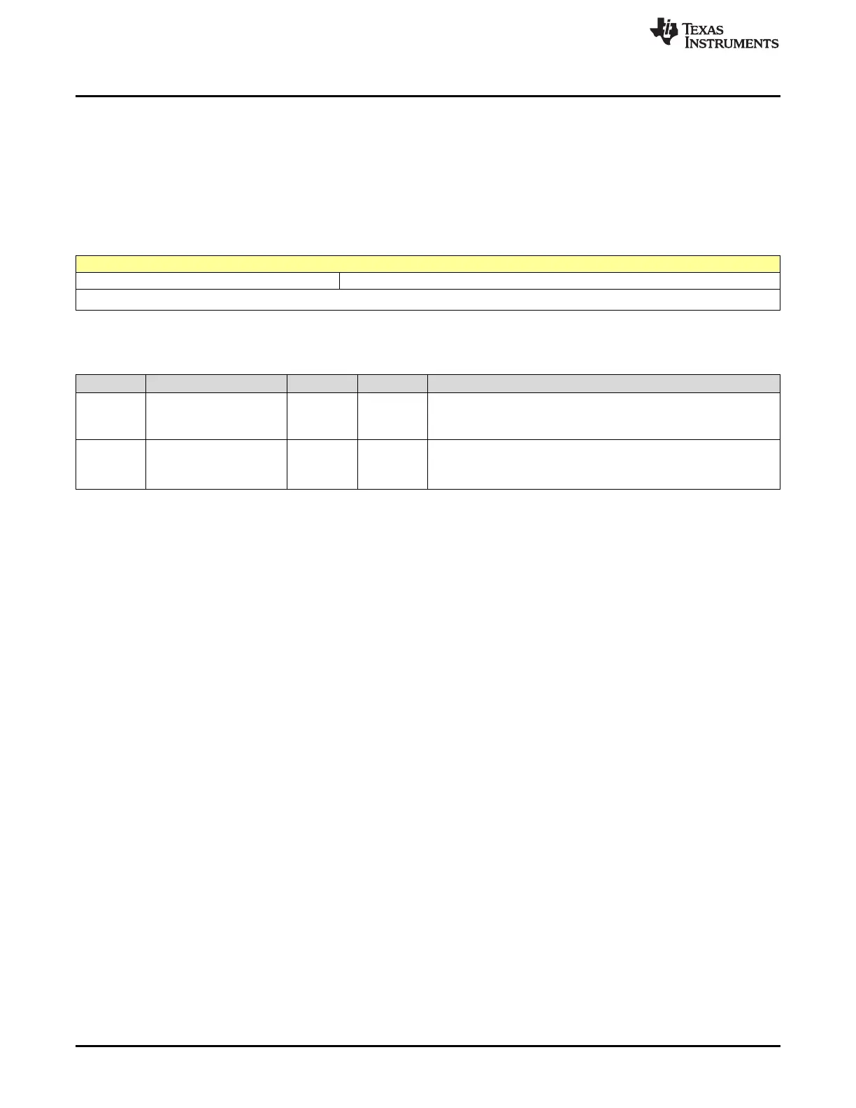
Figure 21-1. FMA Register
31 30 29 28 27 26 25 24 23 22 21 20 19 18 17 16 15 14 13 12 11 10 9 8 7 6 5 4 3 2 1 0
RESERVED OFFSET
R-0h R/W-0h
LEGEND: R/W = Read/Write; R = Read only; W1toCl = Write 1 to clear bit; -n = value after reset
Table 21-2. FMA Register Field Descriptions
Bit Field Type Reset Description
31-20 RESERVED R 0h
Software should not rely on the value of a reserved bit. To provide
compatibility with future products, the value of a reserved bit should
be preserved across a read-modify-write operation.
19-0 OFFSET R/W 0h
Address Offset
Address offset in flash memory where the operation is performed,
except for nonvolatile registers

 Loading...


