www.ti.com
Functional Description
489
SWRU543–January 2019
Submit Documentation Feedback
Copyright © 2019, Texas Instruments Incorporated
Parallel Camera Interface Module
Table 14-1. Image Sensor Interface Signals
Interface Name I/O Description
CAM_P_HS I Row trigger input signal. The polarity of CAM_P_HS can be reversed.
CAM_P_VS I Frame trigger input signal. The polarity of CAM_P_VS can be reversed.
CAM_MCLK I
Input clock used to derive the external clock for the image sensor clock (see
Section 14.3.4).
CAM_XCLK O
External clock for the image sensor module. This clock is derived from the functional
clock (see Section 14.3.4).
CAM_P_DATA [11:4] I
Parallel input data bits. Upper 8 bits of the interface are connected to 8 bits from image
sensor.
CAM_P_CLK I
Latch clock for the parallel input data. The data on the parallel interface are presented
on CAM_P_DATA, one pixel for every CAM_P_CLK rising or falling edge.
14.3 Functional Description
The camera core transfers data from the image sensor into the buffer (FIFO) to generate DMA requests
(one working on the threshold, the other on the remaining data in the FIFO to complete the frame
acquisition).
The camera interface can provide a clock to the external image sensor module (CAM_XCLK). This clock
is derived from the functional clock CAM_MCLK.
14.3.1 Modes of Operation
The camera interface uses the CAM_P_HS and CAM_P_VS signal to detect when the data is valid. This
configuration can work with 8-bit data. No assumptions are made on the data format.
The pixel data is presented on CAM_P_DATA one pixel for every CAM_P_CLK rising edge (or falling,
depending on the configuration of CAM_P_CLK polarity, defined in CC_CTRL.PAR_CLK_POL).
There are additional pixel times between rows that represent a blanking period. The active pixels are
identified by a combination of two additional timing signals: horizontal synchronization (CAM_P_HS) and
vertical synchronization (CAM_P_VS). During the image sensor readout, these signals define when a row
of valid data begins and ends, and when a frame starts and ends. A bit field sets the CAM_P_HS polarity
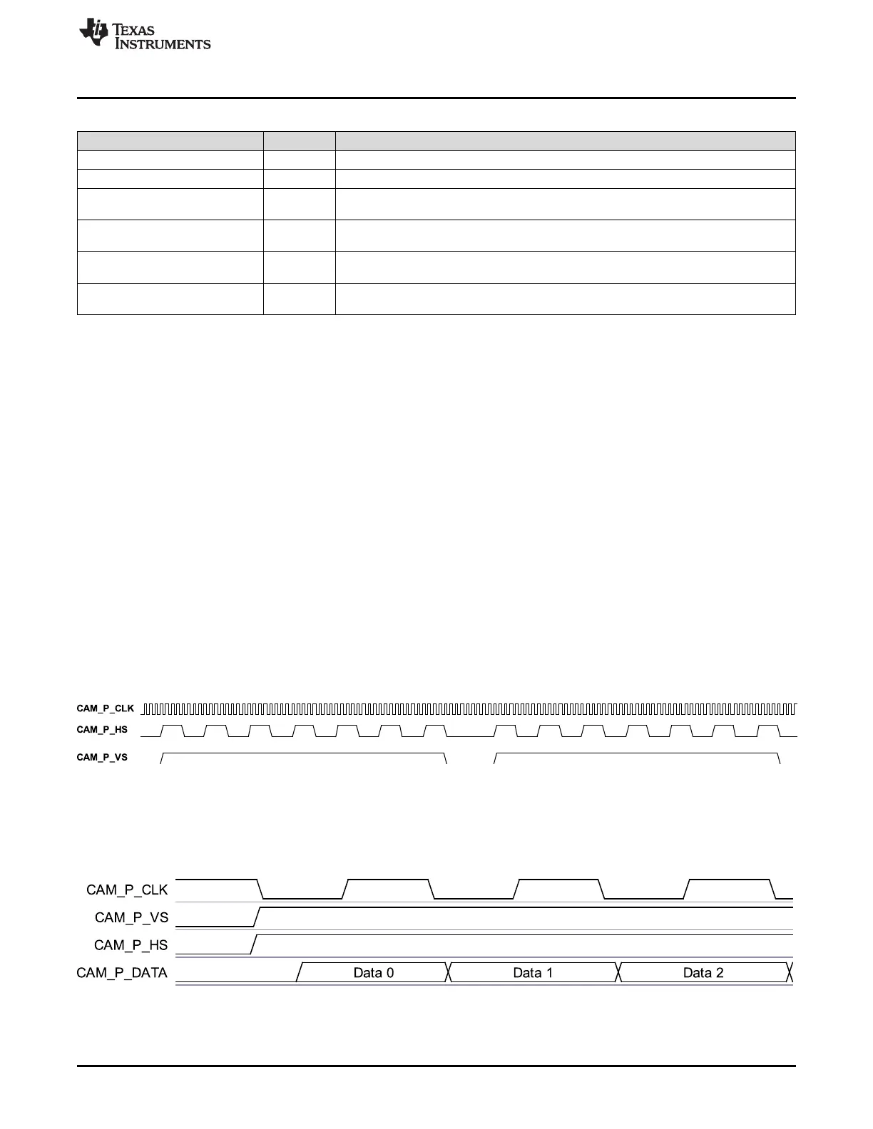
(NOBT_HS_POL) and CAM_P_VS polarity (NOBT_VS_POL). See Figure 14-2.
Figure 14-2. Synchronization Signals and Frame Timing
The clock CAM_P_CLK is running during blanking periods (CAM_P_HS and CAM_P_VS inactive), and at
least 10 clock cycles are required between two consecutive CAM_P_VS active for proper operations when
the line is not a multiple of 12 bytes. Otherwise, one clock cycle is enough to detect CAM_P_VS and work
properly. See Figure 14-3.
Figure 14-3. Synchronization Signals and Data Timing
The acquisition can start either on a beginning of a new frame (CAM_P_VS inactive and then active) or
immediately in function of the CC_CTRL.NOBT_SYNCHRO register bit. Set CC_CTRL.NOBT_SYNCHRO
to 1 to ensure a clean acquisition of the frame.