www.ti.com
SD-HOST Registers
387
SWRU543–January 2019
Submit Documentation Feedback
Copyright © 2019, Texas Instruments Incorporated
SD Host Controller Interface
11.7.10 MMCHS_DATA Register (Offset = 220h) [reset = 0h]
Data register
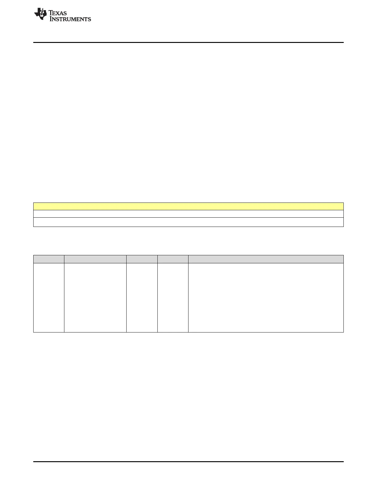
MMCHS_DATA is shown in Figure 11-11 and described in Table 11-14.
Return to Summary Table.
This register is the 32-bit entry point of the buffer for read or write data transfers.
The buffer size is 32 bits × 256 (1024 bytes). Bytes within a word are stored and read in little endian
format. This buffer can be used as two 512-byte buffers to transfer data efficiently without reducing the
throughput. Sequential and contiguous access is necessary to increment the pointer correctly. Random or
skipped access is not allowed. In little endian, if the local host accesses this register byte-wise or 16-bit-
wise, the least significant byte (bits [7:0]) must always be written or read first. The update of the buffer
address is done on the most significant byte write for full 32-bit DATA register, or on the most significant
byte of the last word of block transfer.
Example 1: Byte or 16-bit access
Mbyteen[3:0]=0001 (1-byte) => Mbyteen[3:0]=0010 (1-byte) => Mbyteen[3:0]=1100 (2-bytes) OK
Mbyteen[3:0]=0001 (1-byte) => Mbyteen[3:0]=0010 (1-byte) => Mbyteen[3:0]=0100 (1-byte) OK
Mbyteen[3:0]=0001 (1-byte) => Mbyteen[3:0]=0010 (1-byte) => Mbyteen[3:0]=1000 (1-byte) Bad
Figure 11-11. MMCHS_DATA Register
31 30 29 28 27 26 25 24 23 22 21 20 19 18 17 16 15 14 13 12 11 10 9 8 7 6 5 4 3 2 1 0
DATA
R/W-0h
LEGEND: R/W = Read/Write; R = Read only; W1toCl = Write 1 to clear bit; -n = value after reset
Table 11-14. MMCHS_DATA Register Field Descriptions
Bit Field Type Reset Description
31-0 DATA R/W 0h
Data Register [31:0]
In functional mode (MMCI.MMCHS_CON[4] MODE bit set to the
default value 0):
A read access to this register is allowed only when the buffer read
enable status is set to 1 (MMCi.MMCHS_PSTATE[11] BRE bit),
otherwise a bad access (MMCi.MMCHS_STAT[29] BADA bit) is
signaled.
A write access to this register is allowed only when the buffer write
enable status is set to 1 (MMCi.MMCHS_PSTATE[10] BWE bit),
otherwise a bad access (MMCi.MMCHS_STAT[29] BADA bit) is
signaled and the data is not written.

 Loading...


