www.ti.com
ADC Register Mapping
459
SWRU543–January 2019
Submit Documentation Feedback
Copyright © 2019, Texas Instruments Incorporated
Analog-to-Digital Converter (ADC)
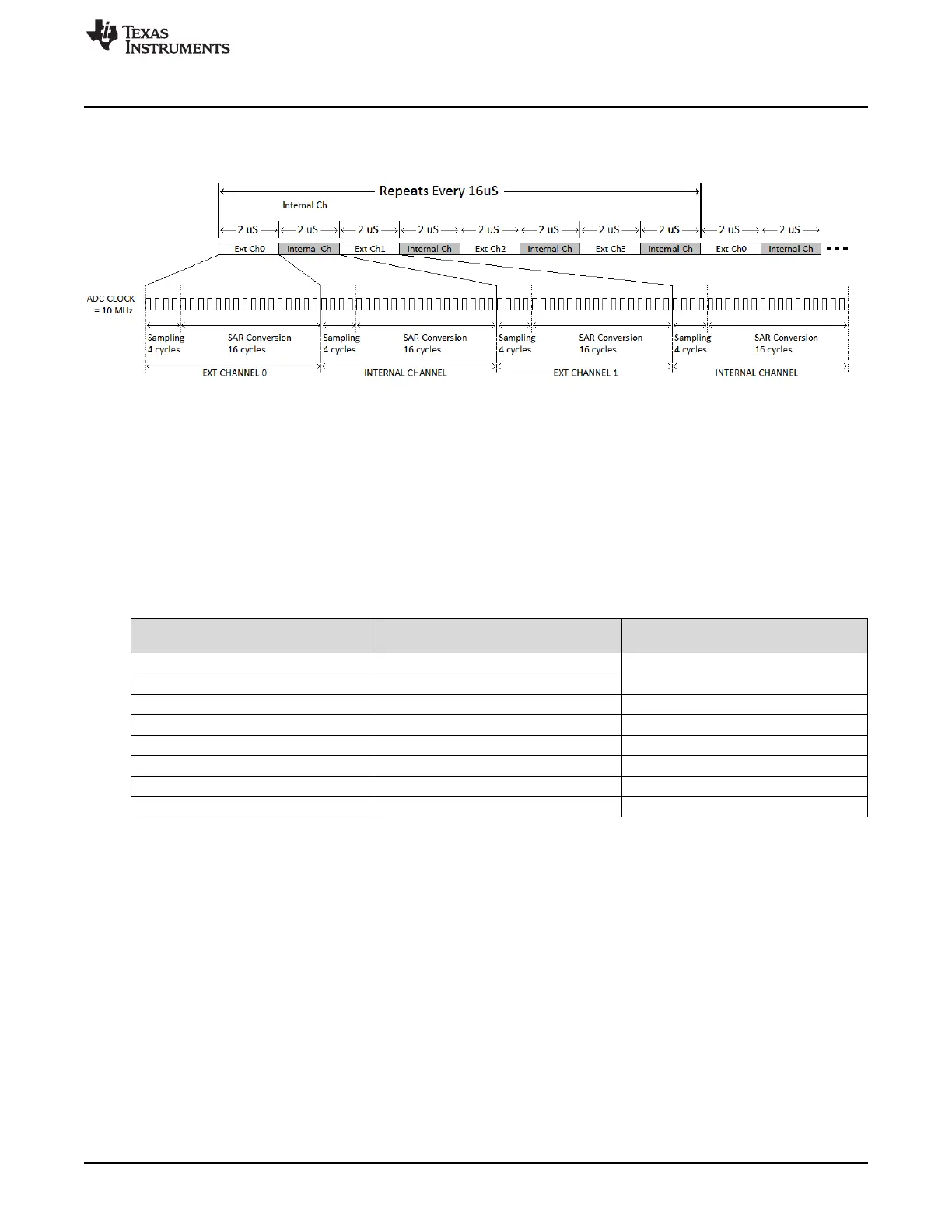
Figure 13-2 shows the round-robin operation of the ADC.
Figure 13-2. Operation of the ADC
13.3 ADC Register Mapping
Naming convention for ADC registers: The CC32xx ADC module supports eight analog input channels:
CH0 to CH7. Each channel is sampled at a fixed rate of 16 µS in a fixed round-robin fashion. See
Figure 13-2.
Out of these, the four channels (even) are available for application processor: CH0, CH2, CH4, CH6.
In the chip pin-mux description, these are referred to as ADC_CH0 to ADC_CH3. Table 13-1 shows the
name aliasing and the convention followed in register description in the following section of this chapter.
Table 13-1. ADC Registers
Pin Number ADC Channel Name Alias in Pin Mux
Channel Name Used In ADC Module
Register Description
57 ADC_CH0 CH0
58 ADC_CH1 CH2
59 ADC_CH2 CH4
60 ADC_CH3 CH6
N/A N/A (Used internal to SoC) CH1
N/A N/A (Used internal to SoC) CH3
N/A N/A (Used internal to SoC) CH5
N/A N/A (Used internal to SoC) CH7
The remaining channels (odd) are used for monitoring various internal levels by the SimpleLink subsystem
in CC32xx SoC. Register bits and functions related to these internal channels are marked as reserved in
the register description. These bits must not be modified by application code to ensure proper functioning
of the system.