www.ti.com
Overview
205
SWRU543–January 2019
Submit Documentation Feedback
Copyright © 2019, Texas Instruments Incorporated
Inter-Integrated Circuit (I
2
C) Interface
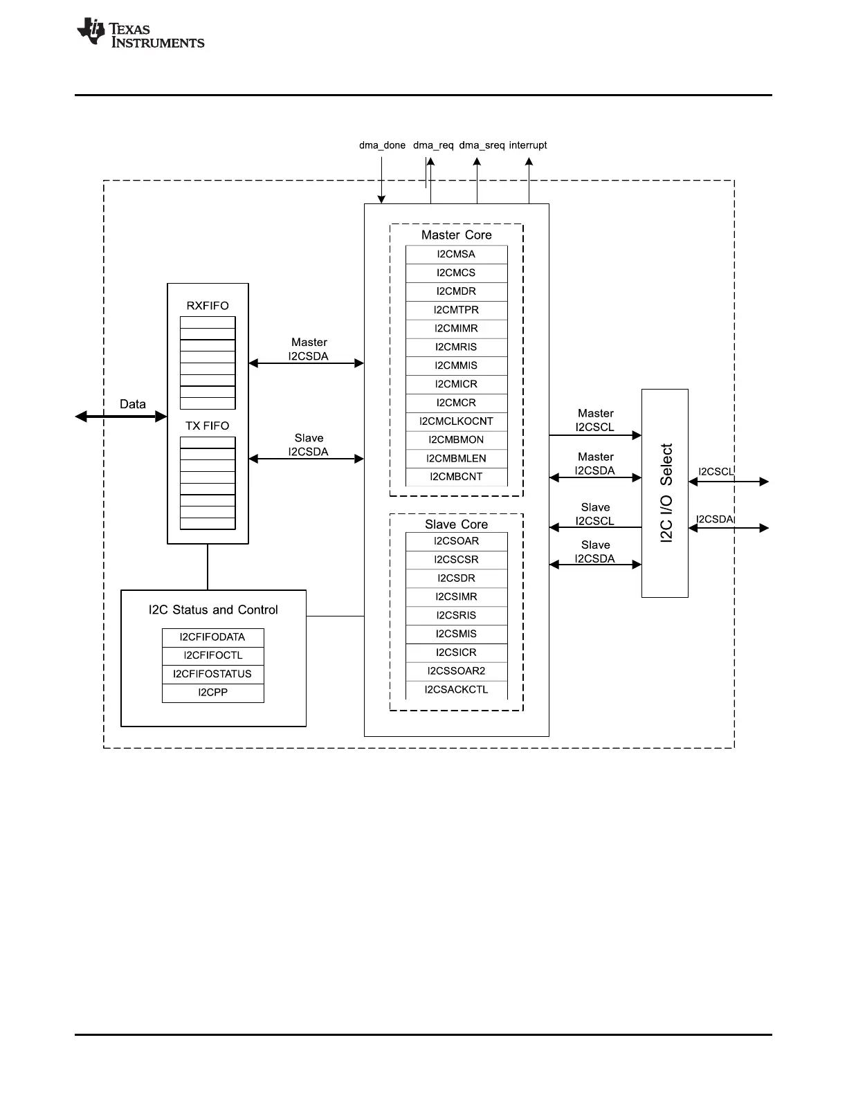
Figure 7-1. I2C Block Diagram
This section describes the details of the architecture of the peripheral and how it is structured. The
architecture and design details are common to all operation modes. Information that is mode-specific to
one of the supported modes can be put in the corresponding supported use case section. This section
describes how the peripheral works.
7.1.2 Signal Description
Table 7-1 lists the external signals of the I
2
C interface and describes the function of each signal. The I
2
C
interface signals are alternate functions for some GPIO signals and default to be GPIO signals at reset.
The pin mux/pin assignment column in Table 7-1 lists the possible GPIO pin placements for the I2C
signals. The CONFMODE bits in the GPIO_PAD_CONFIG register should be set to choose the I2C
function. Set the I2CSDA and I2CSCL pins to open-drain using the IODEN bits of the
GPIO_PAD_CONFIG register.