GPTTRIGSEL
GPTMTAPS
GPTMTAPMR
GPTMTAPR
GPTMTAMATCHR
GPTMTAILR
GPTMTAMR
GPTMTBMR
GPTMTBILR
GPTMTBMATCHR
GPTMTBPR
GPTMTBPMR
GPTMTBPS
Timer A
Free-Running
Output Value
Timer A
Control
TA Comparator
0xFFFF.FFFF (Up Counter Modes, 32-bit)
0x0000.0000 (Down Counter Modes, 32--bit)
0xFFFF (Up Counter Modes, 16--bit)
0x0000 (Down Counter Modes, 16-bit)
Timer A
Interrupt
Timer B
Interrupt
Configuration /
Interrupt
GPTMCFG
GPTMCTL
GPTMSYNC
GPTMIMR
GPTMRIS
GPTMMIS
GPTMICR
GPTMDMAEV
GPTMPP
GPTMCC
GPTMTAR
GPTMTAV
Timer A
Timer B
GPTMTBV
GPTMTBR
Clk/Edge
Detect
Clk/Edge
Detect
Even CCP
Pin
Odd CCP Pin
Timer B
Free-Running
Output Value
Timer B
Control
TB Comparator
0xFFFF.FFFF (Up Counter Modes, 32--bit)
0x0000.0000 (Down Counter Modes, 32-bit)
0xFFFF (Up Counter Modes, 16-bit)
0x0000 (Down Counter Modes, 16-bit)
www.ti.com
Functional Description
307
SWRU543–January 2019
Submit Documentation Feedback
Copyright © 2019, Texas Instruments Incorporated
General-Purpose Timers
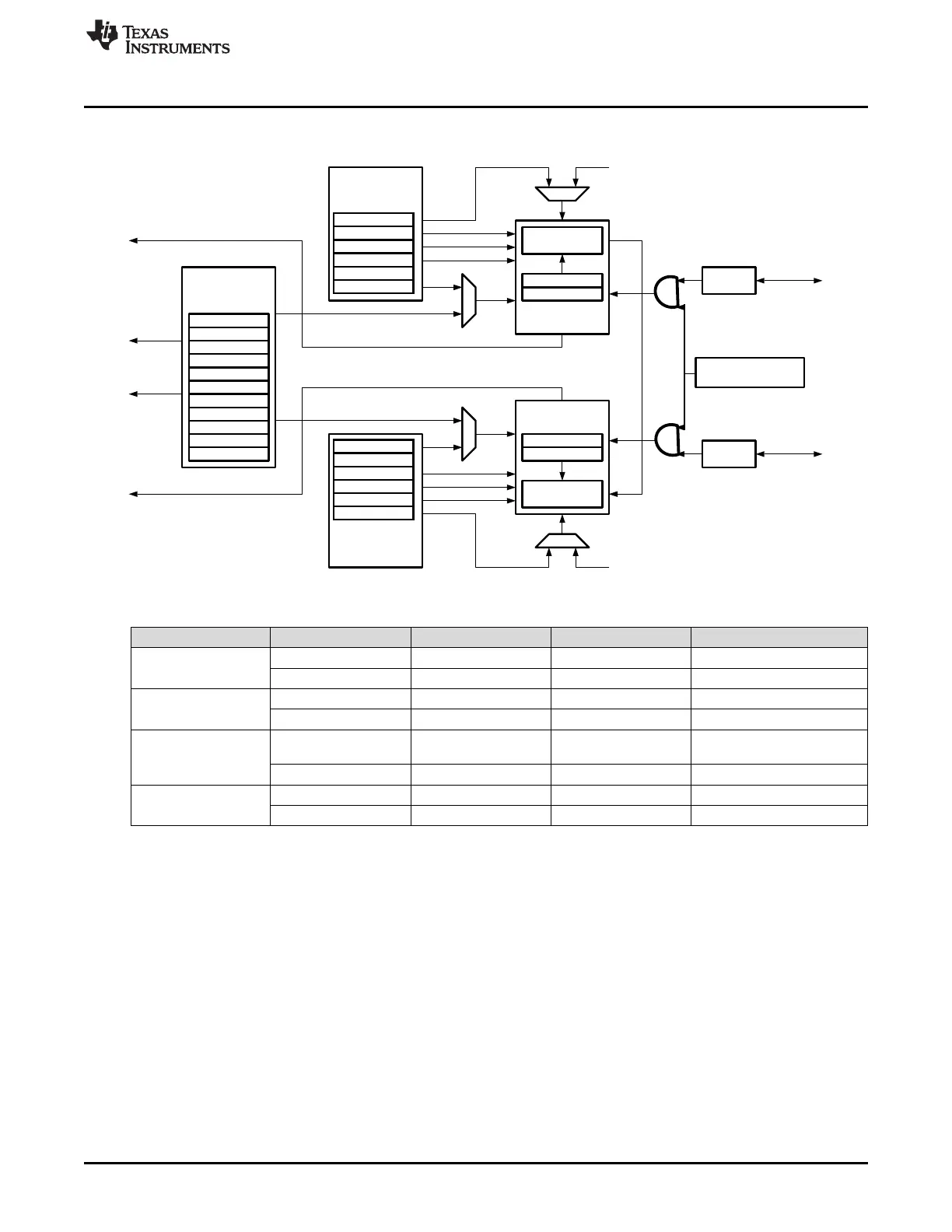
Figure 9-1. GPTM Module Block Diagram
Table 9-1. Available CCP Pins and PWM Outputs/Signals Pins
Timer Up/Down Counter Even CCP Pin Odd CCP Pin PWM Outputs/Signals
16/32-Bit Timer 0
Timer A GT_CCP00 – PWM_OUT0
Timer B – GT_CCP01 PWM_OUT1
16/32-Bit Timer 1
Timer A GT_CCP02 – PWM_OUT2
Timer B – GT_CCP03 PWM_OUT3
16/32-Bit Timer 2
Timer A GT_CCP04 –
OK as is, or add
PWM_OUT4 ?
Timer B – GT_CCP05 PWM_OUT5
16/32-Bit Timer 3
Timer A GT_CCP06 – PWM_OUT6
Timer B – GT_CCP07 PWM_OUT7
The GP timer signals pin-muxed and CONFMODE bits in the GPIO PAD CONFIG register should be set
to choose the GP timer function.
9.3 Functional Description
The main components of each GPTM block follow:
• Two free-running up/down counters (referred to as Timer A and Timer B)
• Two prescaler registers
• Two match registers
• Two prescaler match registers
• Two shadow registers
• Two load/initialization registers and their associated control functions