LF-XOSC
34.768 kHz
RTC
Counter
Comparator
Match
Value Reg
Event Mask
Reg
Event Mask
IO Wakeup
Event Monitor
Edge: Rise/Fall Edge
Level: High/Low
Hibernate
Entry/Exit
StateMachine
RET33 Override
Enable Reg
RET33 Override
Value Reg
OEN33 Override
Value Reg
OEN33 Override
Enable Reg
On Chip PMU
Power Management Unit
V
io
nRESET
Power On
Reset
Controls
Hibernate Entry
Request Reg
Peripheral N
ISO
ISO
ARM® Cortex® -M4Œ
Application Processor
Pin Mux Register
Pad Config Register
High to Low
Level Shifter
High to Low
Level Shifter
High to Low
Level Shifter
Low to High
Level Shifter
Low to High
Level Shifter
High to Low
Level Shifter
High to Low
Level Shifter
Control
Latch
Data Latch
Output
Buffer
DIN
DOUT
DIRECTION
REGISTER I/F
OEN_N
ODI
IDO
Controls
from other pads
(6 wake-capable pads)
OEN33
RET33
PAD
Input
Isolation
PU Enable
PD Enable
Controls
HiZ
Global Control Lines
Connect to All Digital IOs
Hibernate Controller
Pin Mux
REGISTER I/F
Retention Capable GPIO
Vio
(connected to chip input supply. For
example, battery)
On Chip PMU
V
dd_dig
(core logic supply)
ON during LPDs, Off during HIB
OFF During LPDs Sleep mode
V
dd_mcu
(switched logic supply)
OFF during LPDs and HIB
PullUp
PullDown
Peripheral 1
Pin Mapping Recommendations
www.ti.com
606
SWRU543–January 2019
Submit Documentation Feedback
Copyright © 2019, Texas Instruments Incorporated
I/O Pads and Pin Multiplexing
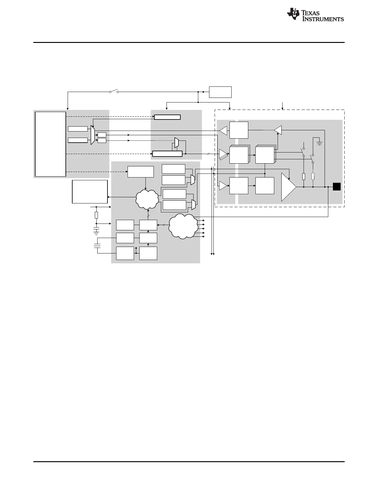
16.8.3 Control Architecture
Figure 16-3 shows the I/O pad data and control path architecture in the CC32xx.
Figure 16-3. I/O Pad Data and Control Path Architecture in CC32xx
16.8.4 CC32xx Pin-mux Examples
Table 16-13 lists recommended pin-out for several application classes.

 Loading...


