www.ti.com
Flash Registers
767
SWRU543–January 2019
Submit Documentation Feedback
Copyright © 2019, Texas Instruments Incorporated
On-Chip Parallel Flash
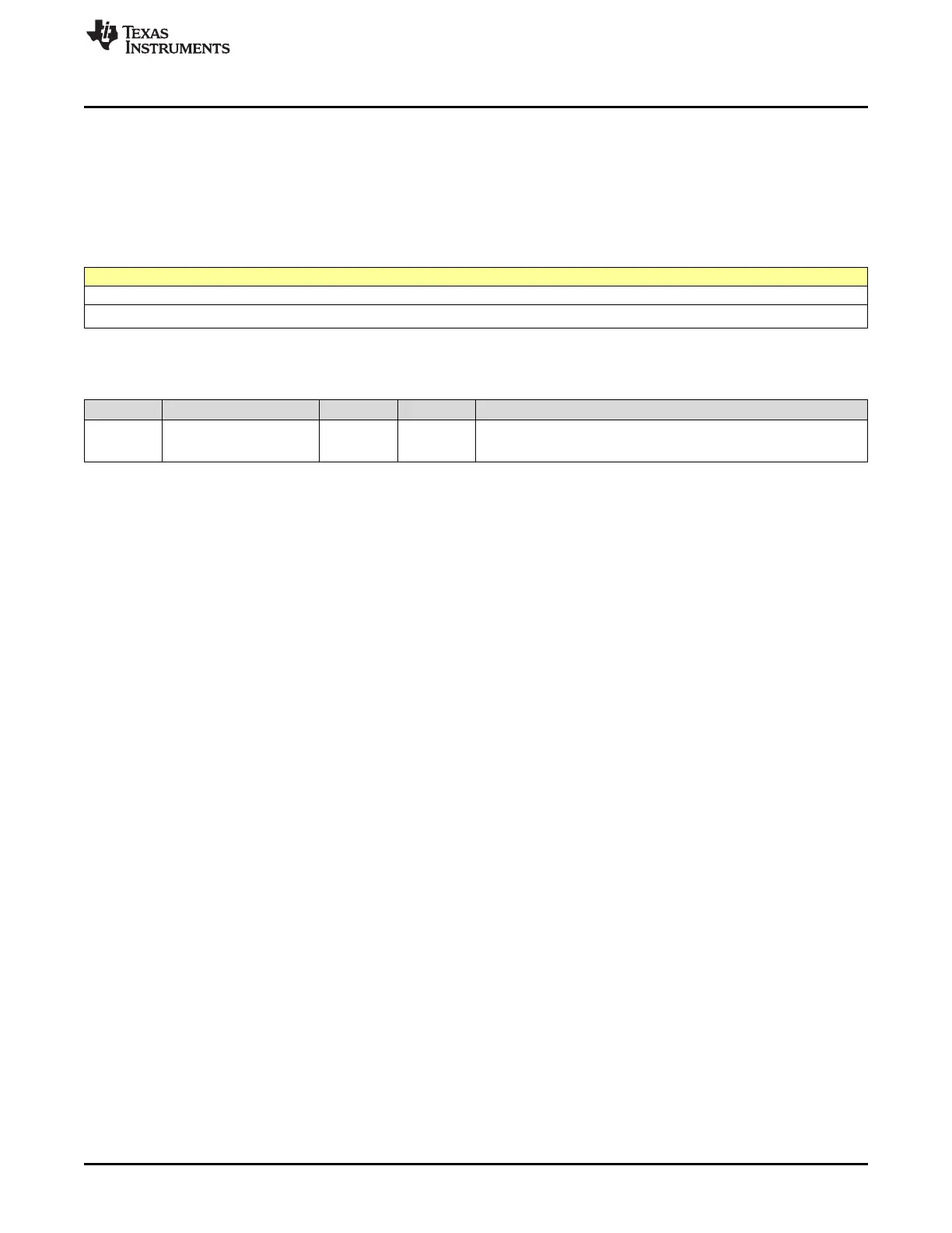
21.5.2 FMD Register (Offset = 4h) [reset = 0h]
FMD is shown in Figure 21-2 and described in Table 21-3.
Return to Summary Table.
This register contains the data to be written during the programming cycle. This register is not used during
erase cycles.
Figure 21-2. FMD Register
31 30 29 28 27 26 25 24 23 22 21 20 19 18 17 16 15 14 13 12 11 10 9 8 7 6 5 4 3 2 1 0
DATA
R/W-0h
LEGEND: R/W = Read/Write; R = Read only; W1toCl = Write 1 to clear bit; -n = value after reset
Table 21-3. FMD Register Field Descriptions
Bit Field Type Reset Description
31-0 DATA R/W 0h
Data Value
Data value for write operation

 Loading...


