Quad Serial Peripheral Interface (QuadSPI)
MPC5606S Microcontroller Reference Manual, Rev. 7
1066 Freescale Semiconductor
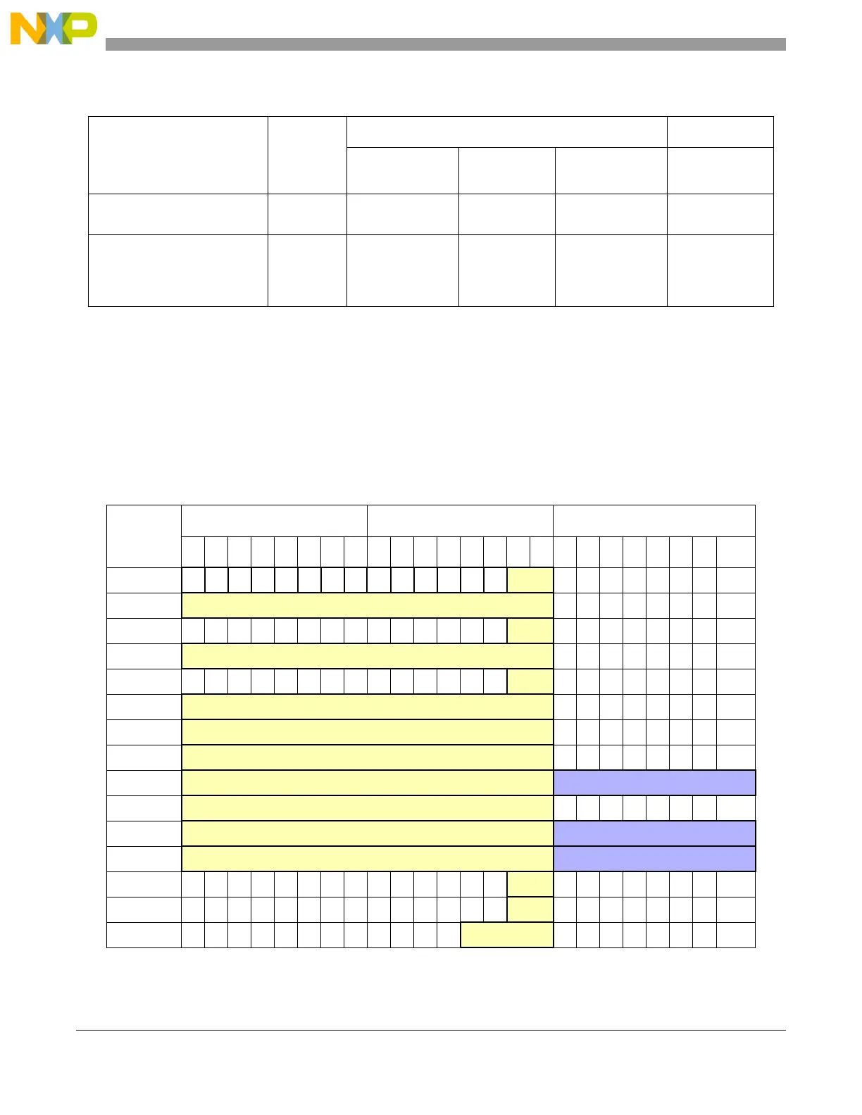
The following table shows only the upper 3 bytes of register QSPI_ICR, byte 0 contains the Instruction
Code. All sizes in Byte 2 are interpreted as the number of bytes, the number of sclk clocks required in the
transaction will be calculated by multiplying with 8 and dividing by number of data lines.
Read Unique ID 4Bh size UniqID63– UniqI
D0
Read JEDEC ID 9Fh size ManID7–ManID0
,
MemID7–Mem0,
CapID7–CapID0
1
Denotes that ‘size’-times one byte is transferred on the serial flash data bus. Total number of bytes must be pro-
vided in the TX Buffer or can be read from the RX Buffer
2
According to Winbond documentation this command only supports a maximum clock speed of 50 MHz. If the
Serial Flash is operated at a higher clock frequency, the clock frequency for this command must be decreased. Refer
to Section 30.7.2, Serial Flash Clock Frequency Limitations, for details.
Table 30-53. Instruction Code Options on Winbond Devices
Instruction
Code
Byte 3 Byte 2 Byte 1
7 6 5 4 3 2 1 0 7 6 5 4 3 2 1 0 7 6 5 4 3 2 1 0
01h Size
02h Size (bytes to be written)
05h Size
32h Size (bytes to be written)
35h Size
03h Size (bytes to be read)
0Bh Size (bytes to be read)
3Bh Size (bytes to be read)
BBh Size (bytes to be read) M7–M0
6Bh Size (bytes to be read)
E3h Size (bytes to be read) M7–M0
EBh Size (bytes to be read) M7–M0
ABh read
1
90h Size
4Bh Size (bytes)
Table 30-52. Winbond Instruction Codes
Command
Instruction
Code
Required Input Data / Parameters Output Data
Options
QSPI_ICR[[ICO]
Address
[QSPI_SFAD]
Data
[TX Buffer]
Status / Data
[RX Buffer]

 Loading...


