Flash Memory
MPC5606S Microcontroller Reference Manual, Rev. 7
Freescale Semiconductor 575
17.2.6.16 User Test 1 register (UT1)
The User Test 1 Register allows to enable the checks on the ECC logic related to the 32 LSB of the Double
Word.
The User Test 1 Register is not accessible whenever MCR.DONE or UT0.AID are low: reading returns
indeterminate data while writing has no effect.
31 AIE: Array Integrity Enable (Read/Write)
AIE set to 1 starts the Array Integrity Check done on all selected and unlocked blocks.
The pattern is selected by AIS, and the MISR (UMISR0-4) can be checked after the operation is complete,
to determine if a correct signature is obtained.
AIE can be set only if MCR.ERS, MCR.PGM and MCR.EHV are all low.
0: Array Integrity Checks, Margin mode, and ECC Logic Checks are not enabled.
1: Array Integrity Checks, Margin mode, and ECC Logic Checks are enabled.
31 AID: Array Integrity Done (Read Only)
AID will be cleared upon an Array Integrity Check being enabled (to signify the operation is on-going).
Once completed, AID will be set to indicate that the Array Integrity Check is complete. At this time the
MISR (UMISR0-4) can be checked.
0: Array Integrity Check is on-going.
1: Array Integrity Check is done.
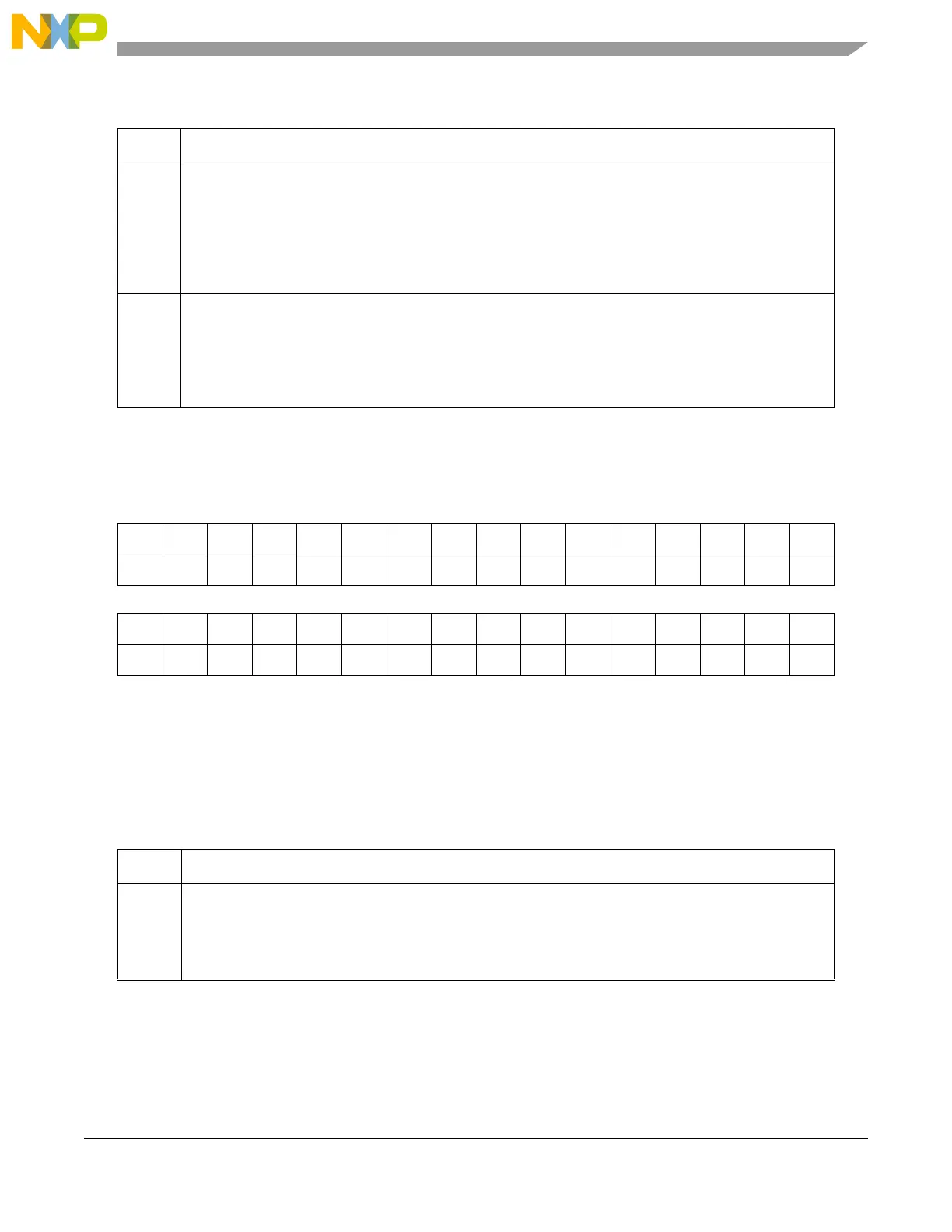
Address Offset: 0x00040 Reset value: 0x00000000
0 1 2 3 4 5 6 7 8 9 10 11 12 13 14 15
DAI31 DAI30 DAI29 DAI28 DAI27 DAI26 DAI25 DAI24 DAI23 DAI22 DAI21 DAI20 DAI19 DAI18 DAI17 DAI16
rw/0 rw/0 rw/0 rw/0 rw/0 rw/0 rw/0 rw/0 rw/0 rw/0 rw/0 rw/0 rw/0 rw/0 rw/0 rw/0
16 17 18 19 20 21 22 23 24 25 26 27 28 29 30 31
DAI15 DAI14 DAI13 DAI12 DAI11 DAI10 DAI09 DAI08 DAI07 DAI06 DAI05 DAI04 DAI03 DAI02 DAI01 DAI00
rw/0 rw/0 rw/0 rw/0 rw/0 rw/0 rw/0 rw/0 rw/0 rw/0 rw/0 rw/0 rw/0 rw/0 rw/0 rw/0
Figure 17-14. User Test 1 register (UT1)
Table 17-24. UT1 field descriptions
Field Description
0:31 DAI31-00: Data Array Input 31-0 (Read/Write)
These bits represent the input of even word of ECC logic used in the ECC Logic Check. The DAI31-00
correspond to the 32 array bits representing Word 0 within the double word.
0: The array bit is forced at 0.
1: The array bit is forced at 1.
Table 17-23. UT0 field descriptions (continued)
Field Description