Clock Description
MPC5606S Microcontroller Reference Manual, Rev. 7
Freescale Semiconductor 223
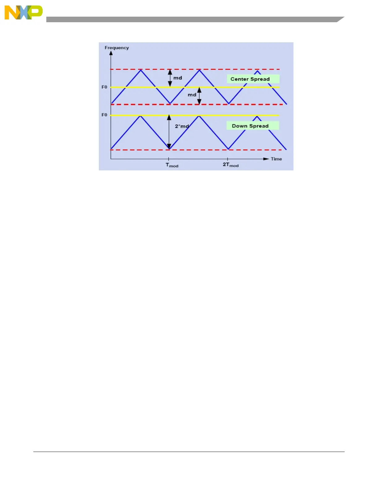
Figure 8-27. PLL frequency modulation modes
8.9.6.4 Powerdown mode
The PLL can be switched off when not required to achieve lower consumption by programming the
registers ME_x_MC register on MC_ME module.
8.9.6.5 1:1 mode (FMPLL0 only)
1:1 mode is set by asserting the mode bit in CR (see Section 8.9.5.1, Control Register (CR)). An external
input signal (mode_en) has been provided to disable this feature. If mode_en is tied to 0, the mode bit in
CR is disabled and there is no way to activate 1:1 mode.
In 1:1 mode the inputs of the PLL are driven by CR and MR, but the division factors and the modulation
parameters have no influence on the output clock. In fact the dividers and the FM control are bypassed
inside the PLL. The PLL output clock (phi) frequency is determined by the following relation:
8.9.7 Recommendations
To avoid any unpredictable behavior of the PLL clock, it is recommended to respect the following
guidelines:
• The PLL VCO frequency should reside in the range 256 MHz to 512 MHz. Care is required when
programming the multiplication and division factors to respect this requirement.
• The user must change the multiplication, division factors only when the PLL output clock is not
selected as system clock. MOD_PERIOD, INC_STEP, SPREAD_SEL bits should be modified
before activating the FM modulated mode. Then strobe has to be generated to enable the new
settings. If STRB_BYP is set to 1 then MOD_PERIOD, INC_STEP and SPREAD_SEL can be
modified only when PLL is in power-down mode.

 Loading...


