System Integration Unit Lite (SIUL)
MPC5606S Microcontroller Reference Manual, Rev. 7
1202 Freescale Semiconductor
37.5.3.10 GPIO Pad Data Output Registers (GPDO0_3–GPDO132_135)
These registers can be used to set or clear a single GPIO pad with a byte access.
The GPIO pad data output registers are a group of 133 one-byte registers used to set or clear the logic value
on their associated pads. Each word contains four registers. The word beginning at Base + 0x0600 contains
GPDO0–GPDO3, the word beginning at Base + 0x0604 contains GPDO3–GPDO07, and so on.
37.5.3.11 GPIO Pad Data Input Registers (GPDI0_3–GPDI132_135)
These registers can be used to read the GPIO pad data with a byte access.
The GPIO pad data input registers are a group of 133 one-byte registers used to set or clear the logic value
on their associated pads. Each word contains four registers. The word beginning at Base + 0x0600 contains
GPDI0–GPDI3, the word beginning at Base + 0x0604 contains GPDI3–GPDI07, and so on.
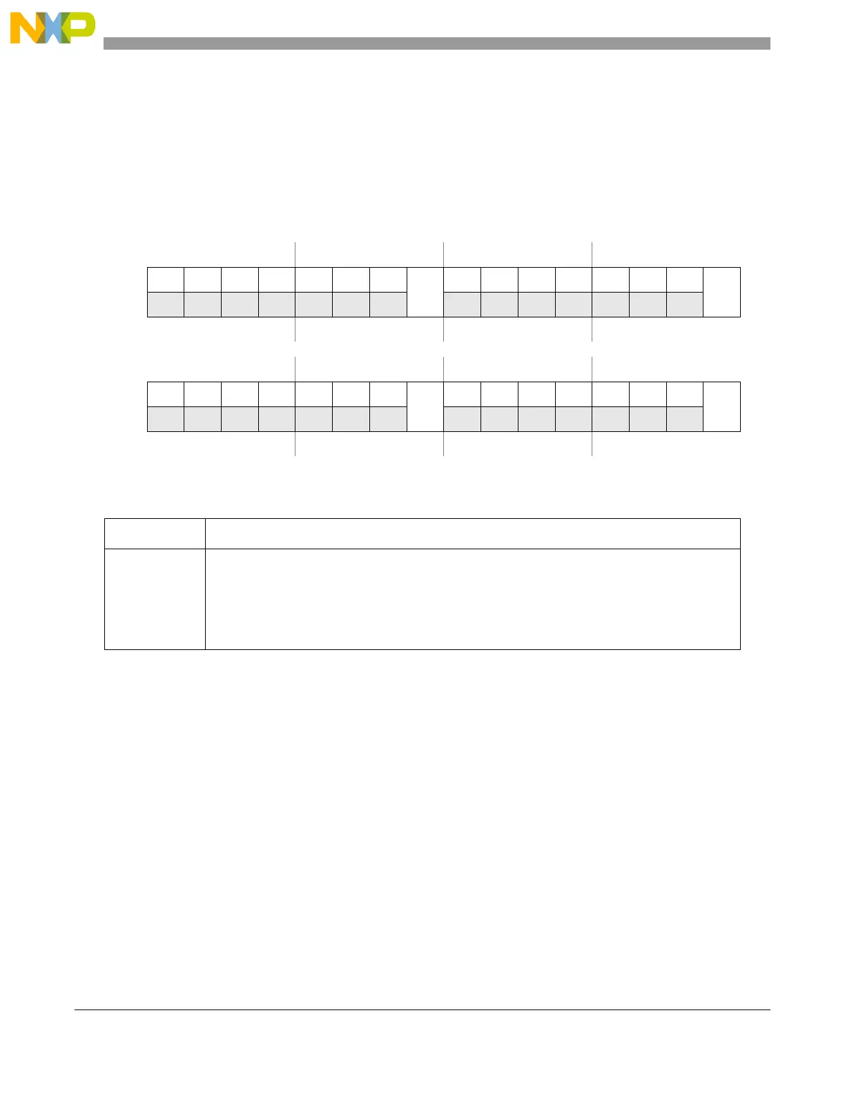
Address: Base + 0x0600–0x0684 (34 registers) Access: User read/write
0 1 2 3 4 5 6 7 8 9 10 11 12 13 14 15
R 0 0 0 0 0 0 0
PDO
[0]
0 0 0 0 0 0 0
PDO
[1]
W
Reset 0 0 0 0 0 0 0 0 0 0 0 0 0 0 0 0
16 17 18 19 20 21 22 23 24 25 26 27 28 29 30 31
R 0 0 0 0 0 0 0
PDO
[2]
0 0 0 0 0 0 0
PDO
[3]
W
Reset 0 0 0 0 0 0 0 0 0 0 0 0 0 0 0 0
Figure 37-13. Port GPIO Pad Data Output register 0–3 (GPDO0_3)
Table 37-13. GPDO field descriptions
Field Description
PDO[x] Pad Data Out
This bit stores the data to be driven out on the external GPIO pad controlled by this register.
0 Logic low value is driven on the corresponding GPIO pad when the pad is configured as an
output
1 Logic high value is driven on the corresponding GPIO pad when the pad is configured as an
output

 Loading...


