Display Control Unit (DCU)
MPC5606S Microcontroller Reference Manual, Rev. 7
434 Freescale Semiconductor
This scenario can also be used in debug mode to calculate the data of the single layer. For such case
CPU has to just enable the single concerned layer and disable all the mathematical function on the
same.
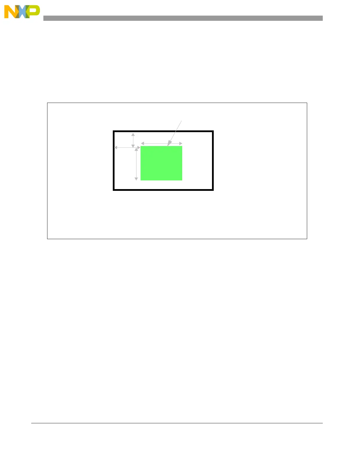
3. CRC can be calculated for the part of the screen as shown in Figure 12-77. Here tag bit is set
low.Data enable is coming for green color portion given in Figure 12-77. Data enable is not
effected by chroma keying. TAG_EN register is low for this case. This can also be used in debug
mode.
Figure 12-77. Safety mode enabled for part of the screen
4. CRC can be calculated only for the safety layers. Layer 0 and 1 can only act as a safety layer. Both
of them have a separate control bits. In calculates the CRC over the intersection of both as shown
(dark pink) in Figure 12-78. Here tag bit set high for all the bits corresponding to the layer 0 and 1
as shown by pink color (both dark and light) as shown in Figure 12-78. Also data is affected by
chroma keying.Tag bit is cleared for the pixel removed by chroma keying.As shown in
Figure 12-78 Data enable is controlled by the region shown in green color and tag is controlled by
the pink region. CRC is calculated over region in dark pink.
LenX
StartX
StartY
area of concern
LenY
Note: Enable to CRC is sent for the
Green Portion

 Loading...


