RM0046 Flash Memory
Doc ID 16912 Rev 5 315/936
Note: To perform program and erase operations, the control registers in the actual referenced
Flash array must both be programmed, but the configuration of the platform Flash controller
module is defined by the platform Flash controller control registers of code array0.
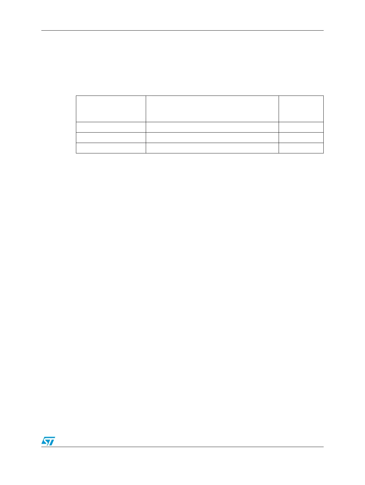
The 32-bit memory map for the platform Flash controller control registers is shown in
Table 138.
17.2.5 Functional description
The platform Flash controller interfaces between the AHB-Lite 2.v6 system bus and the
Flash memory arrays.
The platform Flash controller generates read and write enables, the Flash array address,
write size, and write data as inputs to the Flash array. The platform Flash controller captures
read data from the Flash array interface and drives it onto the AHB. As much as four pages
of data (128-bit width) from bank0 are buffered by the platform Flash controller. Lines may
be prefetched in advance of being requested by the AHB interface, allowing single-cycle (0
AHB wait states) read data responses on buffer hits.
Several prefetch control algorithms are available for controlling page read buffer fills.
Prefetch triggering may be restricted to instruction accesses only, data accesses only, or
may be unrestricted. Prefetch triggering may also be controlled on a per-master basis.
Buffers may also be selectively enabled or disabled for allocation by instruction and data
prefetch.
Access protections may be applied on a per-master basis for both reads and writes to
support security and privilege mechanisms.
Throughout this discussion, bkn_ is used as a prefix to refer to two signals, each for each
bank: bk0_ and bk1_. Also, the nomenclature Bx_Py_RegName is used to reference a
program-visible register field associated with bank “x” and port “y”.
17.2.6 Basic interface protocol
The platform Flash controller interfaces to the Flash array by driving addresses
(bkn_fl_addr[23:0]) and read or write enable signals (bkn_fl_rd_en, bkn_fl_wr_en).
The read or write enable signal (bkn_fl_rd_en, bkn_fl_wr_en) is asserted in conjunction with
the reference address for a single rising clock when a new access request is made.
Addresses are driven to the Flash array in a flow-through fashion to minimize array access
time. When no outstanding access is in progress, the platform Flash controller drives
addresses and asserts bkn_fl_rd_en or bkn_fl_wr_en and then may change to the next
outstanding address in the next cycle.
Table 138. Platform Flash controller 32-bit memory map
Offset from
PFlash_BASE
(0xFFE8_8000)
Register Location
0x001C Platform Flash Configuration Register 0 (PFCR0) on page 17-353
0x0020 Platform Flash Configuration Register 1 (PFCR1) on page 17-357
0x0024 Platform Flash Access Protection Register (PFAPR) on page 17-359