Voltage Regulators and Power Supplies RM0046
838/936 Doc ID 16912 Rev 5
34.1.4 Registers Description
Voltage Regulator Control Register (VREG_CTL)
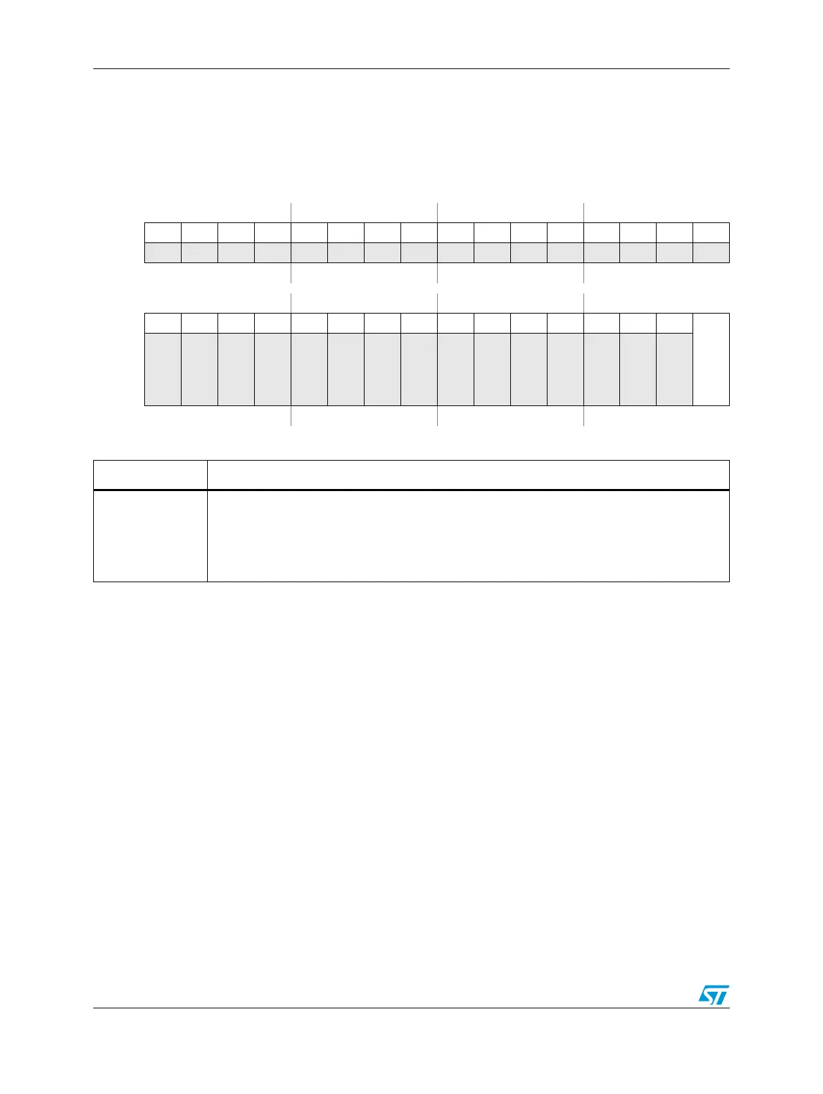
Figure 495. Voltage Regulator Control register (VREG_CTL)
Address:
Base + 0x0080 Access: User read/write
0123456789101112131415
R00000000 00000 000
W
Reset0000000000000000
16 17 18 19 20 21 22 23 24 25 26 27 28 29 30 31
R000000010000000
5V_LVD_MASK
W
Reset0000000100000001
Table 452. VREG_CTL field descriptions
Field Description
5V_LVD_MASK
Mask bit for 5 V LVD from regulator
This is a read/write bit and must be unmasked by writing a 1 by software to generate LVD
functional reset request to RGM for 5V trip.
05 V LVD not masked
15 V LVD masked