Functional Safety RM0046
738/936 Doc ID 16912 Rev 5
27.2.2 Features
The register protection module includes these features:
● Restrict write accesses for the module under protection to supervisor mode only
● Lock registers for first 6 KB of memory-mapped address space
● Address mirror automatically sets corresponding lock bit
● Once configured lock bits can be protected from changes
27.2.3 Modes of operation
The register protection module is operable when the module under protection is operable.
27.2.4 External signal description
There are no external signals.
27.2.5 Memory map and registers description
This section provides a detailed description of the memory map of a module using the
Register protection. The original 16 KB module memory space is divided into five areas as
shown in Figure 419.
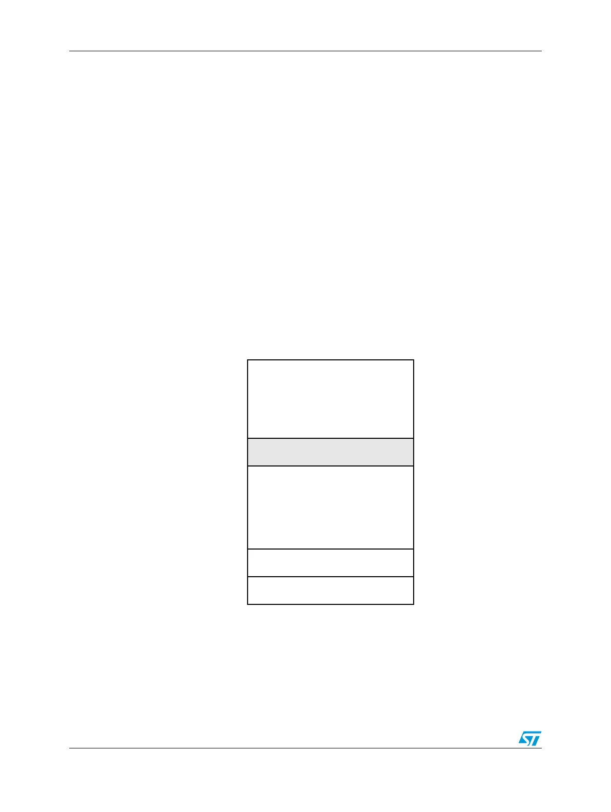
Figure 419. Register protection memory diagram
Area 1 is 6 KB and holds the normal functional module registers and is transparent for all
read/write operations.
Area 2, 2 KB starting at address 0x1800, is reserved.
module register space
Base + 0x0000
6 KB
2 KB Reserved
mirror module register space
6 KB
1.5 KB Lock Bits
with user defined
Base + 0x1800
Base + 0x2000
Base + 0x3800
soft locking function
512 Bytes Configuration
Base + 0x3E00
Base + 0x3FFF
Area 1
Area 2
Area 3
Area 4
Area 5