Deserial Serial Peripheral Interface (DSPI) RM0046
472/936 Doc ID 16912 Rev 5
Modified SPI transfer format (MTFE = 1, CPHA = 0)
In this modified transfer format both the master and the slave sample later in the SCK period
than in classic SPI mode to allow for delays in device pads and board traces. These delays
become a more significant fraction of the SCK period as the SCK period decreases with
increasing baud rates.
Note: For the modified transfer format to operate correctly, you must thoroughly analyze the SPI
link timing budget.
The master and the slave place data on the SOUT_x pins at the assertion of the CSx signal.
After the CSx to SCK_x delay has elapsed the first SCK_x edge is generated. The slave
samples the master SOUT_x signal on every odd numbered SCK_x edge. The slave also
places new data on the slave SOUT_x on every odd numbered clock edge.
The master places its second data bit on the SOUT_x line one system clock after odd
numbered SCK_x edge. The point where the master samples the slave SOUT_x is selected
by writing to the SMPL_PT field in the DSPIx_MCR. Table 2 28 lists the number of system
clock cycles between the active edge of SCK_x and the master sample point for different
values of the SMPL_PT bit field. The master sample point can be delayed by one or two
system clock cycles.
Figure 222 shows the modified transfer format for CPHA = 0. Only the condition where
CPOL = 0 is illustrated. The delayed master sample points are indicated with a lighter
shaded arrow.
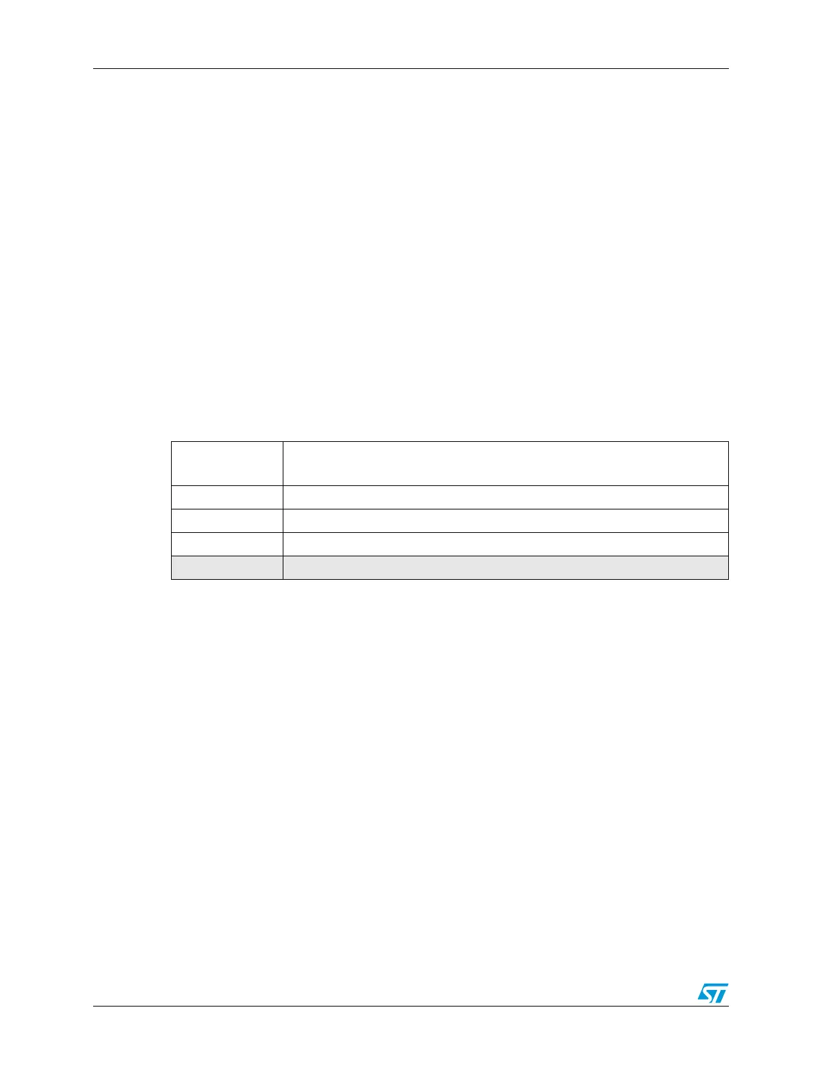
Table 228. Delayed master sample point
SMPL_PT
Number of system clock cycles between odd-numbered edge of SCK
and sampling of SIN
00 0
01 1
10 2
11 Invalid value