FlexPWM RM0046
692/936 Doc ID 16912 Rev 5
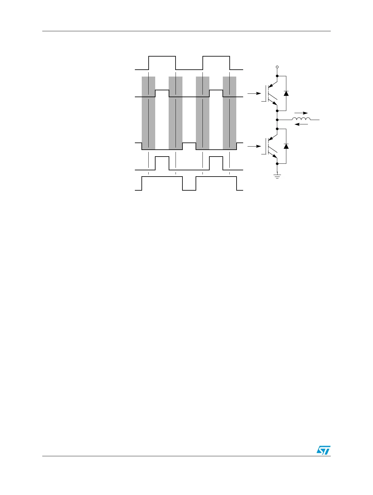
Figure 378. Deadtime distortion
During deadtime, load inductance distorts output voltage by keeping current flowing through
the diodes. This deadtime current flow creates a load voltage that varies with current
direction. With a positive current flow, the load voltage during deadtime is equal to the
bottom supply, putting the top transistor in control. With a negative current flow, the load
voltage during deadtime is equal to the top supply putting the bottom transistor in control.
Remembering that the original PWM pulse widths where shortened by deadtime insertion,
the averaged sinusoidal output will be less than the desired value. However, when deadtime
is inserted, it creates a distortion in the motor current waveform. This distortion is
aggravated by dissimilar turn-on and turn-off delays of each of the transistors. By giving the
PWM module information on which transistor is controlling at a given time this distortion can
be corrected.
For a typical circuit in complementary channel operation, only one of the transistors will be
effective in controlling the output voltage at any given time. This depends on the direction of
the motor current for that pair. See Figure 379. To correct distortion one of two different
factors must be added to the desired PWM value, depending on whether the top or bottom
transistor is controlling the output voltage. Therefore, the software is responsible for
calculating both compensated PWM values prior to placing them in the VALx registers.
Either the VAL2/VAL3 or the VAL4/VAL5 register pair controls the pulse width at any given
time. For a given PWM pair, whether the VAL2/VAL3 or VAL4/VAL5 pair is active depends on
either:
● The state of the current status pin, PWMx, for that driver
● The state of the odd/even correction bit, IPOL, for that driver
Desired
Deadtime
PWM to top
Positive
Negative
PWM to bottom
Positive current
Negative current
load voltage
transistor
transistor
load voltage
load voltage
current
current
V+