Clock Description RM0046
104/936 Doc ID 16912 Rev 5
Modulation Register (MR)
i_lock
This bit is set by hardware whenever there is a lock/unlock event.It is cleared by software, writing
1.
s_lock
This bit indicates whether the PLL has acquired lock.
0: PLL unlocked
1: PLL locked
pll_fail_mask
This bit masks the pll_fail output.
0: pll_fail not masked
1: pll_fail masked
pll_fail_flag
This bit is asynchronously set by hardware whenever a loss of lock event occurs while PLL is
switched on. It is cleared by software, writing 1.
Table 13. CR field descriptions (continued)
Field Description
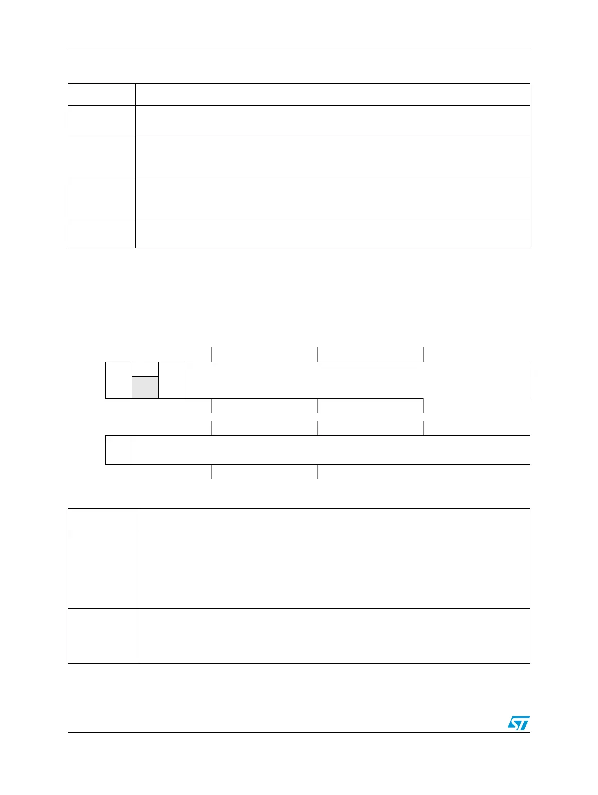
Figure 16. Modulation Register (MR)
Address:
Base + 0x0004
Access: Supervisor read/write
User read-only
0123456789101112131415
R
STRB
_BYPA
SS
0
SPRD
_SEL
MOD_PERIOD
W
Reset0000000000000000
16 17 18 19 20 21 22 23 24 25 26 27 28 29 30 31
R
FM_
EN
INC_STEP
W
Reset0000000000000000
Table 14. MR field descriptions
Field Description
STRB_BYPASS
Strobe bypass
The STRB_BYPASS signal bypasses the STRB signal used inside the PLL to latch the correct
values for control bits (INC_STEP, MOD_PERIOD and SPRD_SEL).
0: STRB latches the PLL modulation control bits.
1: STRB is bypassed. In this case, the control bits need to be static. The control bits must be
changed only when PLL is in power down mode.
SPRD_SEL
Spread type selection
The SPRD_SEL bit selects the spread type in Frequency Modulation mode.
0: Center spread
1: Down spread