Flash Memory RM0046
352/936 Doc ID 16912 Rev 5
Address Register (ADR)
The Address Register provides the first failing address in the event module failures (ECC,
RWW, or FPEC) or the first address at which a ECC single error correction occurs.
Table 153. LMS field descriptions
Field Description
0:13
Reserved (Read Only)
A write to these bits has no effect. A read of these bits always outputs 0.
14:15 Reserved
LSL[15:0]
16:31
Low Address Space Block Select 15–0
A value of 1 in the select register signifies that the block is selected for erase.
A value of 0 in the select register signifies that the block is not selected for erase. The reset value
for the select register is 0, or unselected.
For code Flash, LSL[5:0] are related to sectors B0F[5:0], respectively. See Table 142 for more
information.
For data Flash, LSL[3:0] are related to sectors B1F[3:0], respectively. See Ta bl e 143 for more
information.
The blocks must be selected (or unselected) before doing an erase interlock write as part of the
Erase sequence. The select register is not writable once an interlock write is completed or if a
high voltage operation is suspended.
In the event that blocks are not present (due to configuration or total memory size), the
corresponding LSL bits will default to unselected, and will not be writable. The reset value will
always be 0, and register writes will have no effect.
In the code Flash macrocell, bits LSL[15:6] are read-only and locked at 0.
In the data Flash macrocell, bits LSL[15:4] are read-only and locked at 0.
0 Low Address Space Block is unselected for Erase.
1 Low Address Space Block is selected for Erase.
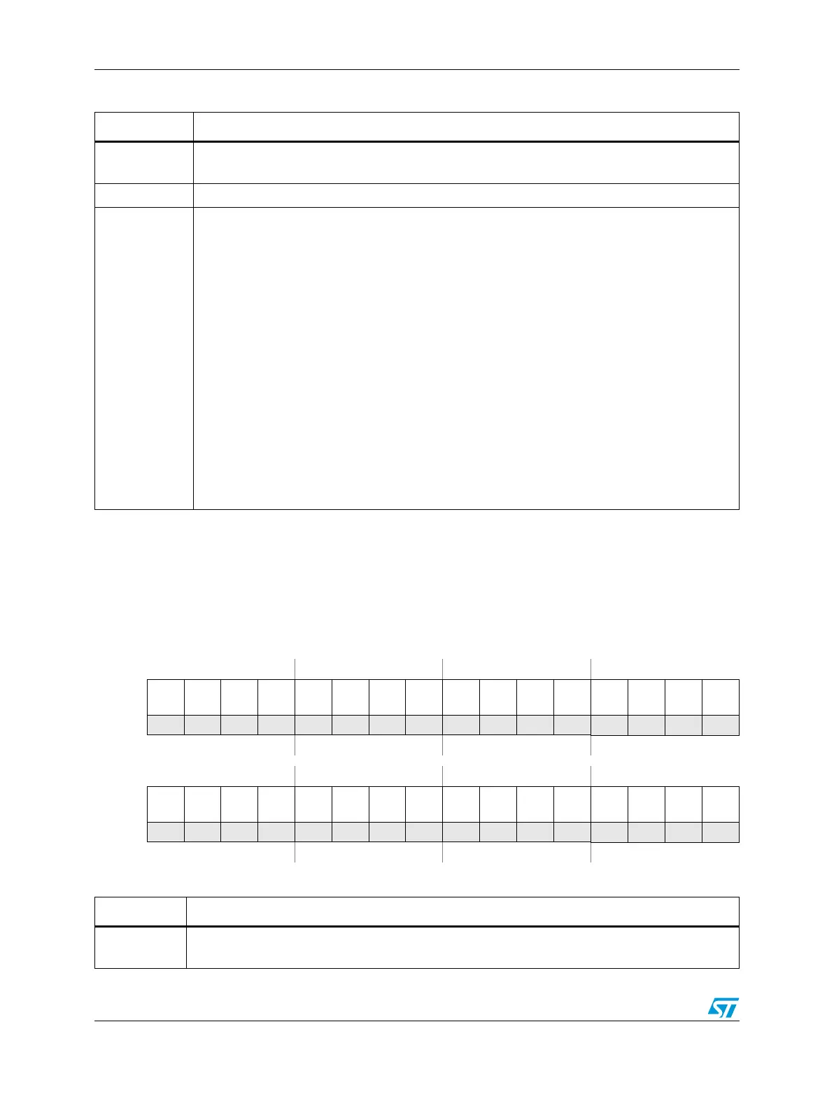
Figure 159. Address Register (ADR)
Address:
Base + 0x0018 Access: User read/write
0123456789101112131415
R00000000 0
AD
22
AD
21
AD
20
AD
19
AD
18
AD
17
AD
16
W
Reset0000000000000000
16 17 18 19 20 21 22 23 24 25 26 27 28 29 30 31
R
AD
15
AD
14
AD
13
AD
12
AD
11
AD
10
AD
9
AD
8
AD
7
AD
6
AD
5
AD
4
AD
3
000
W
Reset0000000000000000
Table 154. ADR field descriptions
Field Description
0:8
Reserved (Read Only)
A write to these bits has no effect. A read of these bits always outputs 0.