RM0046 SPC560P40/34 memory map
Doc ID 16912 Rev 5 69/936
2 SPC560P40/34 memory map
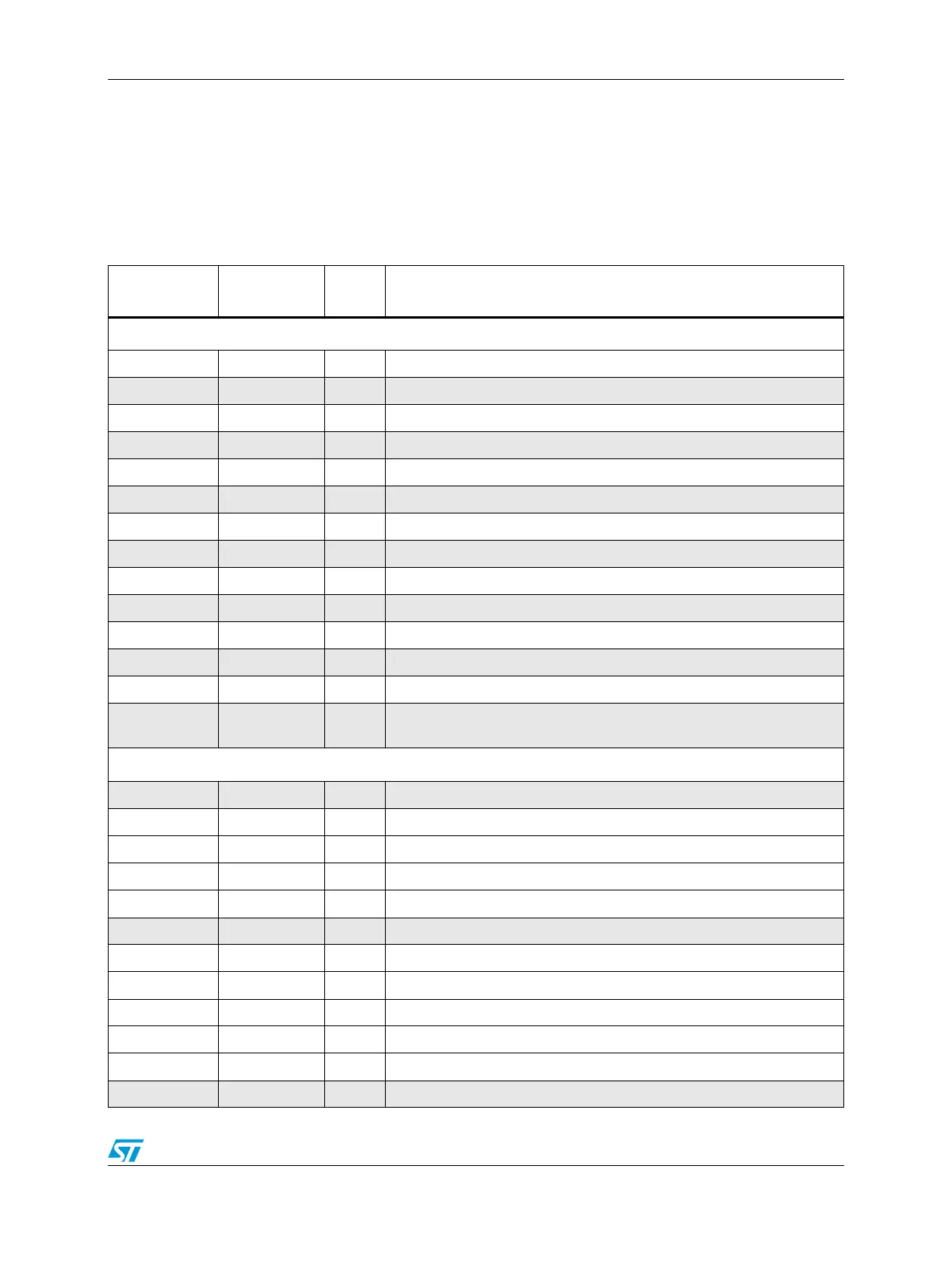
Table 3 shows the memory map for the SPC560P40/34. All addresses on the
SPC560P40/34, including those that are reserved, are identified in the table. The addresses
represent the physical addresses assigned to each IP block.
Table 3. Memory map
Start address End address
Size
(KB)
Region name
On-chip memory
0x0000_0000 0x0003_FFFF 256 Code Flash Array 0
0x0004_0000 0x001F_FFFF 1792 Reserved
0x0020_0000 0x0020_3FFF 16 Code Flash Array 0 Shadow Sector
0x0020_4000 0x003F_FFFF 2032 Reserved
0x0040_0000 0x0040_3FFF 16 Code Flash Array 0 Test Sector
0x0040_4000 0x007F_FFFF 4080 Reserved
0x0080_0000 0x0080_FFFF 64 Data Flash Array 0
0x0081_0000 0x00C0_1FFF 4040 Reserved
0x00C0_2000 0x00C0_3FFF 8 Data Flash Array 0 Test Sector
0x00C0_4000 0x00FF_FFFF 4080 Reserved
0x0100_0000 0x1FFF_FFFF 507904 Flash Emulation Mapping
0x2000_0000 0x3FFF_FFFF 524288 Reserved
0x4000_0000 0x4000_4FFF 20 SRAM
0x4000_5000 0xC3F8_0000
104853
6
Reserved
On-chip peripherals
0xC3F8_0000 0xC3F8_7FFF 32 Reserved
0xC3F8_8000 0xC3F8_BFFF 16 Code Flash 0 Configuration (CFLASH_0)
0xC3F8_C000 0xC3F8_FFFF 16 Data Flash 0 Configuration (DFLASH_0)
0xC3F9_0000 0xC3F9_3FFF 16 System Integration Unit Lite (SIUL)
0xC3F9_4000 0xC3F9_7FFF 16 WakeUp Unit (WKUP)
0xC3F9_8000 0xC3FD_7FFF 256 Reserved
0xC3FD_8000 0xC3FD_BFFF 16 System Status and Configuration Module (SSCM)
0xC3FD_C000 0xC3FD_FFFF 16 Mode Entry module (ME)
0xC3FE_0000 0xC3FE_3FFF 16 Clock Generation Module (CGM, XOSC, IRC, FMPLL_0, CMU0)
0xC3FE_4000 0xC3FE_7FFF 16 Reset Generation Module (RGM)
0xC3FE_8000 0xC3FE_BFFF 16 Power Control Unit (PCU)
(1)
0xC3FE_C000 0xC3FE_FFFF 16 Reserved