RM0046 Analog-to-Digital Converter (ADC)
Doc ID 16912 Rev 5 583/936
23.3.4 ADC CTU (Cross Triggering Unit)
Overview
The ADC cross triggering unit (CTU) is added to enhance the injected conversion capability
of the ADC. The CTU contains multiple event inputs that can be used to select the channels
to be converted from the appropriate event configuration register. The CTU generates a
trigger output pulse of one clock cycle and outputs onto an internal data bus the channel to
be converted. A single channel is converted for each request. After performing the
conversion, the ADC returns the result on internal bus.
The conversion result is also saved in the corresponding data register and it is compared
with watchdog thresholds if requested.
The CTU can be enabled by setting MCR[CTUEN].
The CTU and the ADC are synchronous with the MC_PLL_CLK in both cases.
CTU in control mode
In CTU control mode, the CPU is able to write in the ADC registers but it cannot start any
conversion. Conversion requests can be generated only by the CTU trigger pulse. If a
normal or injected conversion is requested, it is automatically discarded.
When a CTU trigger pulse is received with the injected channel number, the conversion
starts. The CTUSTART bit is set automatically at this point and it is also automatically reset
when CTU Control mode is disabled (CTUEN = ‘0’).
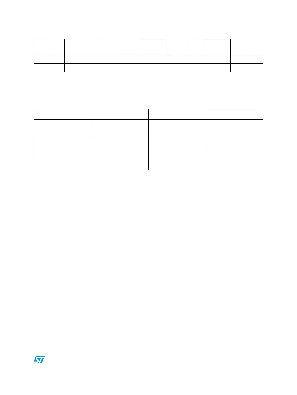
16 0.063 9 1 0.500 8.000 1 0.625 0 1.188 19.000
32 0.031 17 1 0.500 16.000 2 0.625 1 1.156 37.000
1. Where: INPSAMPLE 3
2. Where: INPSAMP 6, N = 0.5; INPSAMP > 6, N = 1
3. Where: T
sample
= (INPSAMP-N)T
ck
; Must be 500 ns
Table 290. ADC sampling and conversion timing at 5 V / 3.3 V for ADC0 (continued)
Clock
(MHz)
T
ck
(s)
INPSAMPLE
(1)
Ndelay
(2)
T
sample
(3)
T
sample
/T
ck
INPCMP
T
eval
(s)
INPLATCH
T
conv
(s)
T
conv
/
T
ck
Table 291. Max/Min ADC_clk frequency and related configuration settings at 5 V / 3.3 V for ADC0
INPCMP INPLATCH Max f
ADC_clk
Min f
ADC_clk
00/01
020+4%6
1——
10
0——
132+4%6
11
0——
132+4%9