RM0046 Clock Generation Module (MC_CGM)
Doc ID 16912 Rev 5 135/936
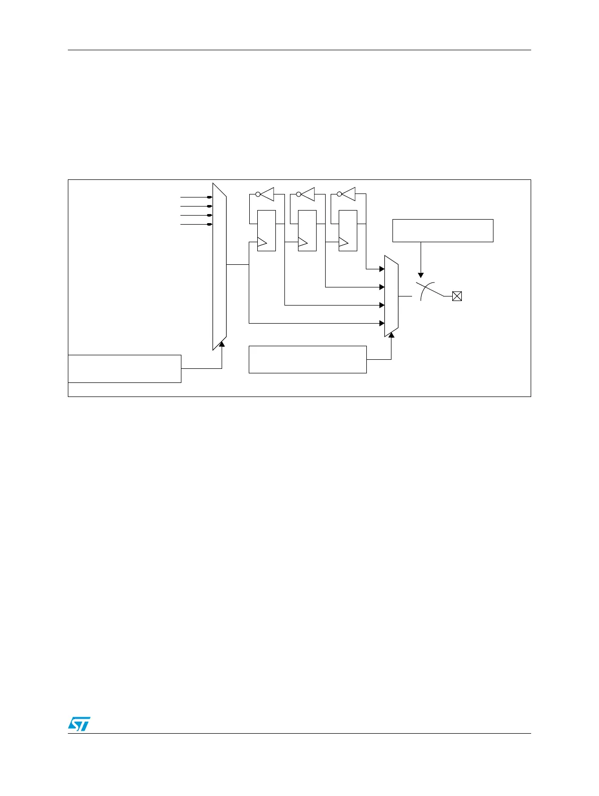
5.10 Output Clock Multiplexing
The MC_CGM contains a multiplexing function for a number of clock sources which can
then be used as output clock sources. The selection is done via the CGM_OCDS_SC
register.
5.11 Output Clock Division Selection
Figure 41. MC_CGM Output Clock Multiplexer and PAD[22] Generation
The MC_CGM provides the following output signals for the output clock generation:
● PA D [ 2 2 ] ( s e e Figure 41). This signal is generated by using one of the 3-stage ripple
counter outputs or the selected signal without division. The non-divided signal is not
guaranteed to be 50% duty cycle by the MC_CGM.
the MC_CGM also has an output clock enable register (see Section 5.5.1, “Output Clock
Enable Register (CGM_OC_EN)) which contains the output clock enable/disable control bit.
CGM_OCDS_SC.SELCTL
CGM_OCDS_SC.SELDIV
0
1
2
3
Register
Register
16 MHz int. RC osc. 0
4 MHz crystal osc. 1
system PLL 2
reserved 3
PAD[22]
’0’
CGM_OC_EN Register