RM0046 Flash Memory
Doc ID 16912 Rev 5 371/936
All the sectors of the Flash module belong to the same partition (Bank), therefore when a
Modify operation is active on some sectors, no read access is possible on any other sector
(Read-While-Modify is not supported).
During a Flash modify operation, any attempt to read any Flash location will output invalid
data and the MCR[RWE] bit will be automatically set. This means that the Flash block is not
fetchable when a modify operation is active and these commands must be executed from
another memory (internal RAM or another Flash block).
If a reset occurs during a modify operation, the operation is interrupted and the block is reset
to read mode. The data integrity of the Flash section where the modify operation has been
terminated is not guaranteed. The interrupted Flash modify operation must be repeated.
In general, each modify operation is started through a sequence of three steps:
1. The first instruction selects the desired operation by setting its corresponding selection
bit in MCR (MCR[PGM] or MCR[ERS]) or UT0 (UT0[MRE] or UT0[EIE]).
2. The second step defines the operands: the address and the data for programming or
the sectors for erase or margin read.
3. The third instruction starts the modify operation by setting MCR[EHV] or UT0[AIE].
Once selected, but not yet started, one operation can be canceled by resetting the operation
selection bit.
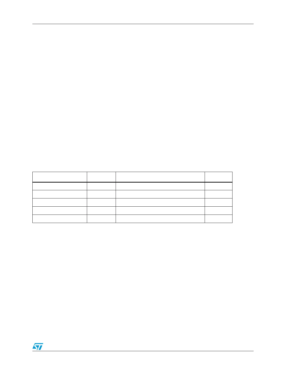
A summary of the available Flash modify operations are shown in Tabl e 1 7 2 .
Once MCR[EHV] (or UT0[AIE]) is set, the operands cannot be modified until MCR[DONE]
(or UT0[AID]) is high.
In general, each modify operation is completed through a sequence of four steps:
1. Wait for operation completion: wait for bit MCR[DONE] (or UT0[AID]) to go high.
2. Check operation result: check bit MCR[PEG] (or compare UMISR0–4 with expected
value).
3. Switch off FPEC by resetting MCR[EHV] (or UT0[AIE]).
4. Deselect current operation by clearing MCR[PGM] and MCR[ERS] (or UT0[MRE] and
UT0[EIE]).
If a modify operation is on-going in one of the Flash blocks, it is forbidden to start any other
modify operation on the other Flash block.
In the following sections, all the possible modify operations are described and some
examples of the sequences needed to activate them are presented.
Table 172. Flash modify operations
Operation Select bit Operands Start bit
Double word program MCR[PGM] Address and data by interlock writes MCR[EHV]
Sector erase MCR[ERS] LMS MCR[EHV]
Array integrity check None LMS UT0[AIE]
Margin read UT0[MRE] UT0[MRV] + LMS UT0[AIE]
ECC logic check UT0[EIE] UT0[DSI], UT1, UT2 UT0[AIE]