FlexPWM RM0046
696/936 Doc ID 16912 Rev 5
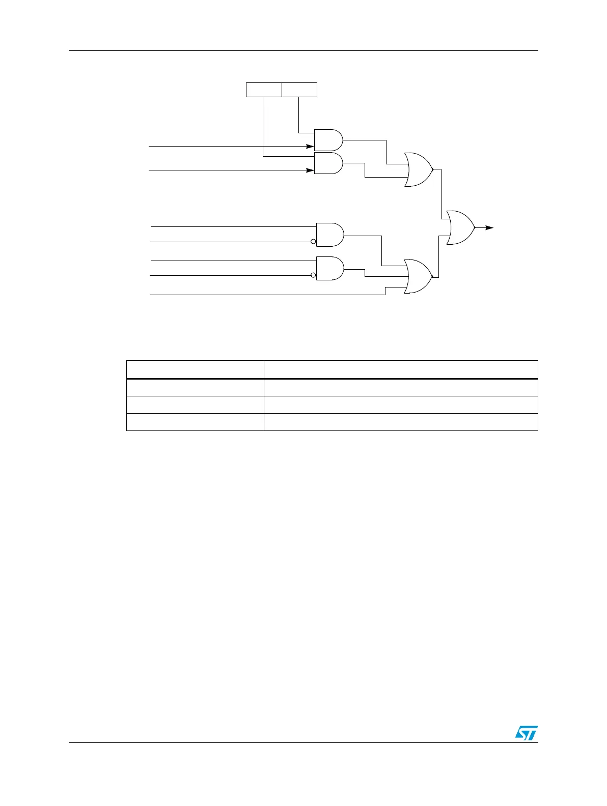
Figure 382. Fault decoder for PWMA
25.8.13 Fault pin filter
Each fault pin has a programmable filter that can be bypassed. The sampling period of the
filter can be adjusted with the FILT_PER field of the FFILTx register. The number of
consecutive samples that must agree before an input transition is recognized can be
adjusted using the FILT_CNT field of the same register. Setting FILT_PER to all 0 disables
the input filter for a given FAULTx pin.
Upon detecting a logic 0 on the filtered FAULTx pin (or a logic 1 if FLVLx is set), the
corresponding FFPINx and fault flag, FFLAGx, bits are set. The FFPINx bit remains set as
long as the filtered FAULTx pin is zero. Clear FFLAGx by writing a logic 1 to FFLAGx.
If the FIEx, FAULTx pin interrupt enable bit is set, the FFLAGx flag generates a CPU
interrupt request. The interrupt request latch remains set until:
● Software clears the FFLAGx flag by writing a logic one to the bit
● Software clears the FIEx bit by writing a logic zero to it
● A reset occurs
Even with the filter enabled, there is a combinational path from the FAULTx inputs to the
PWM pins. This logic is also capable of holding a fault condition in the event of loss of clock
to the PWM module.
DISA0DISA1
Disable
FAULT0
FAULT1
PWMA
Wait/Halt Mode
WAITEN
Debug Mode
DBGEN
Stop Mode
Table 361. Fault mapping
PWM pin Controlling register bits
PWMA DISA[1:0]
PWMB DISB[1:0]
PWMX DISX[1:0]