Flash Memory RM0046
328/936 Doc ID 16912 Rev 5
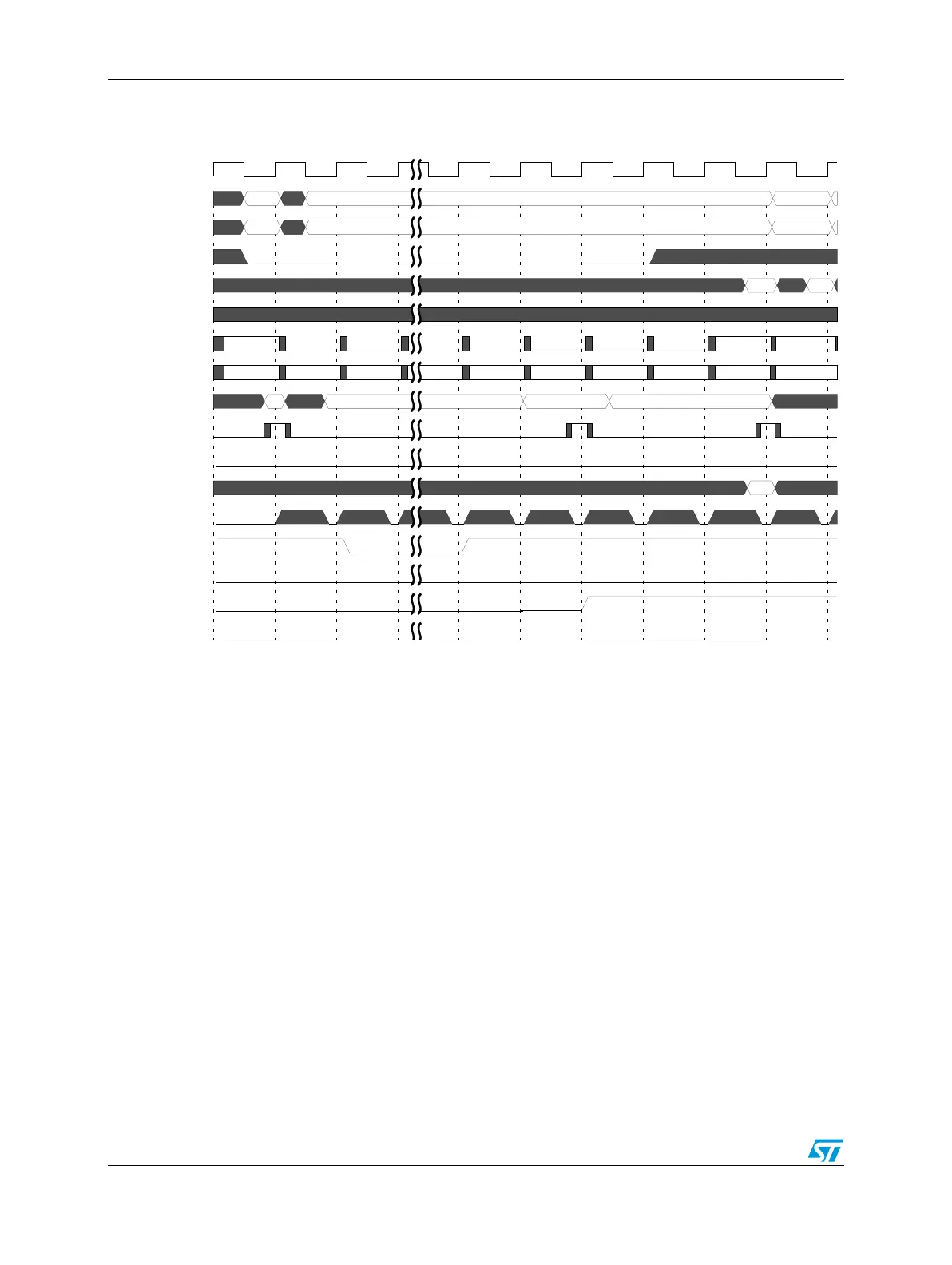
Figure 149. 3-cycle access, stall-and-retry with BKn_RWWC = 11x
As shown in Figure 149, the 3-cycle access to address y is interrupted when an operation
causes the bkn_done signal to be negated, signaling that the array bank is busy with a high-
voltage program or erase event. Eventually, this array operation completes (at the end of
cycle 4) and bkn_done returns to a logical 1. In cycle 6, the platform Flash controller module
retries the read to address y that was interrupted by the negation of bkn_done in cycle 3.
Note that throughout cycles 2–9, the AHB bus pipeline is stalled with a read to address y in
the AHB data phase and a read to address y + 4 in the address phase. Depending on the
state of the least-significant-bit of the BKn_RWWC control field, the hardware may also
signal a stall notification interrupt (if BKn_RWWC = 110). The stall notification interrupt is
shown as the optional assertion of ECSM’s MIR[FBnSI] (Flash bank n stall interrupt).
nonseq
seq
addr y
addr y+4
C(y)
C(y+4)
okay
okay
okay okay okay okay okay okay
y
C(y)
Burst Read, Stall-and-Retry, APC = 2, RWSC = 2, PFLM = 2
123456
7
8
addr y
seq
addr y+8
y+16
y+16
y
okay
okay
addr y+16addr y (retry)
hclk
htrans
haddr, hprot
hwrite
hrdata
hwdata
hready_out
hresp
bkn_fl_addr
bkn_fl_rd_en
bkn_fl_wr_en
bkn_fl_rdata
bkn_fl_xfr_err
bkn_done
bkn_abort
ecsm_mir[fbnsi]
ecsm_mir[fbnai]
9
10