Deserial Serial Peripheral Interface (DSPI) RM0046
444/936 Doc ID 16912 Rev 5
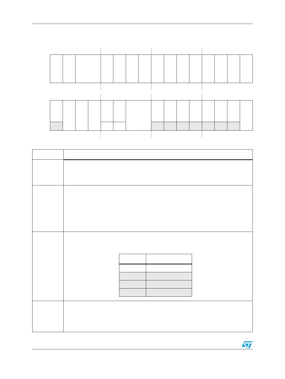
Figure 207. DSPI Module Configuration Register (DSPIx_MCR)
Address:
Base + 0x0000 Access: User read/write
0123456789101112131415
R
MSTR
CONT_SCKE
DCONF[0:1]
FRZ
MTFE
PCSSE
ROOE
PCSIS7
PCSIS6
PCSIS5
PCSIS4
PCSIS3
PCSIS2
PCSIS1
PCSIS0
W
Reset0000000000000000
16 17 18 19 20 21 22 23 24 25 26 27 28 29 30 31
R0
MDIS
DIS_TXF
DIS_RXF
CLR_TXF
CLR_RXF
SMPL_PT[0:1]
0000000
HALT
W w1c w1c
Reset0000000000000001
Table 206. DSPIx_MCR field descriptions
Field Description
0
MSTR
Master/slave mode select
Configures the DSPI for master mode or slave mode.
0 DSPI is in slave mode.
1 DSPI is in master mode.
1
CONT_SCKE
Continuous SCK enable
Enables the serial communication clock (SCK) to run continuously. Refer to Section 20.8.6,
“Continuous Serial communications clock for details.
0 Continuous SCK disabled
1 Continuous SCK enabled
If the FIFO is enabled with continuous SCK mode, before setting the CONT_SCKE bit, the TX-FIFO should
be cleared and only CTAR0 register should be used for transfer attributes otherwise a change in SCK
frequency occurs.
2–3
DCONF
[0:1]
DSPI configuration
The following table lists the DCONF values for the various configurations.
4
FRZ
Freeze
Enables the DSPI transfers to be stopped on the next frame boundary when the device enters
debug mode.
0 Do not halt serial transfers.
1 Halt serial transfers.
DCONF Configuration
00 SPI
01 Invalid value
10 Invalid value
11 Invalid value