RM0046 Clock Generation Module (MC_CGM)
Doc ID 16912 Rev 5 131/936
5.5.10 Auxiliary Clock 2 Divider Configuration Register (CGM_AC2_DC0)
This register controls the auxiliary clock 2 divider.
5.6 Functional Description
5.7 System Clock Generation
Figure 37 shows the block diagram of the system clock generation logic. The MC_ME
provides the system clock select and switch mask (see MC_ME chapter for more details),
and the MC_RGM provides the safe clock request (see MC_RGM chapter for more details).
The safe clock request forces the selector to select the 16 MHz int. RC osc. as the system
clock and to ignore the system clock select.
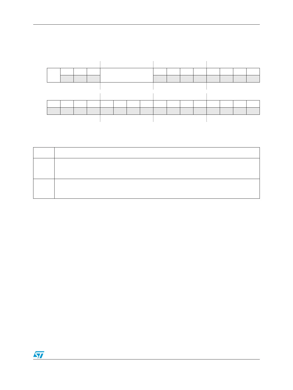
Figure 36. Auxiliary Clock 2 Divider Configuration Register (CGM_AC2_DC0)
Address 0xC3FE_0394 Access: User read, Supervisor read/write, Test read/write
0123456789101112131415
R
DE0
000
DIV0
00000000
W
Reset1000000000000000
16 17 18 19 20 21 22 23 24 25 26 27 28 29 30 31
R0000000000000000
W
Reset0000000000000000
Table 35. Auxiliary Clock 2 Divider Configuration Register (CGM_AC2_DC0) Field Descriptions
Field Description
DE0
Divider 0 Enable
0 Disable auxiliary clock 2 divider 0
1 Enable auxiliary clock 2 divider 0
DIV0
Divider 0 Division Value — The resultant (unused) will have a period DIV0 + 1 times that of auxiliary
clock 2. If the DE0 is set to 0 (Divider 0 is disabled), any write access to the DIV0 field is ignored and the
(unused) remains disabled.