RM0046 Deserial Serial Peripheral Interface (DSPI)
Doc ID 16912 Rev 5 469/936
Equation 26
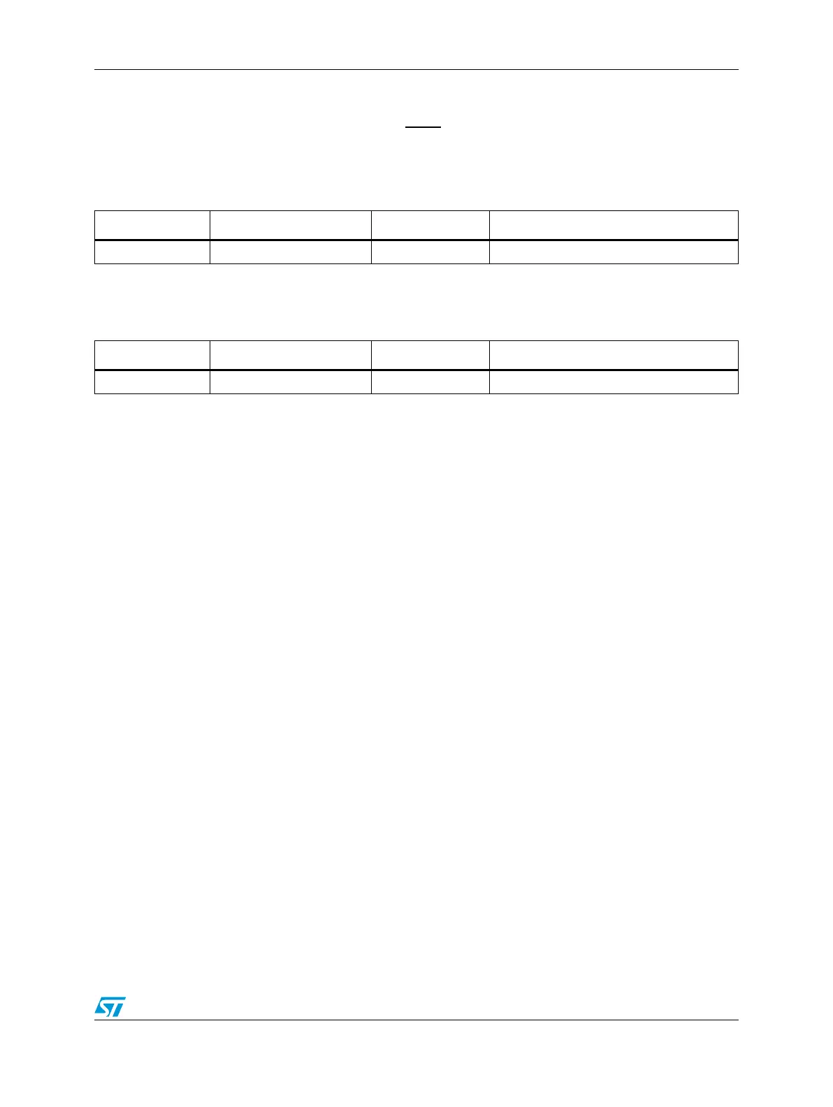
Table 226 shows an example of the computed t
PCSSCK
delay.
Table 227 shows an example of the computed the t
PASC
delay.
20.8.5 Transfer formats
The SPI serial communication is controlled by the serial communications clock (SCK_x)
signal and the CSx signals. The SCK_x signal provided by the master device synchronizes
shifting and sampling of the data by the SIN_x and SOUT_x pins. The CSx signals serve as
enable signals for the slave devices.
When the DSPI is the bus master, the CPOL and CPHA bits in the DSPI clock and transfer
attributes registers (DSPIx_CTARn) select the polarity and phase of the serial clock, SCK_x.
The polarity bit selects the idle state of the SCK_x. The clock phase bit selects if the data on
SOUT_x is valid before or on the first SCK_x edge.
When the DSPI is the bus slave, CPOL and CPHA bits in the DSPIx_CTAR0 (SPI slave
mode) select the polarity and phase of the serial clock. Even though the bus slave does not
control the SCK signal, clock polarity, clock phase and number of bits to transfer must be
identical for the master device and the slave device to ensure proper transmission.
The DSPI supports four different transfer formats:
● Classic SPI with CPHA = 0
● Classic SPI with CPHA = 1
● Modified transfer format with CPHA = 0
● Modified transfer format with CPHA = 1
A modified transfer format is supported to allow for high-speed communication with
peripherals that require longer setup times. The DSPI can sample the incoming data later
than halfway through the cycle to give the peripheral more setup time. The MTFE bit in the
DSPIx_MCR selects between classic SPI format and modified transfer format. The classic
SPI formats are described in Section , “Classic SPI transfer format (CPHA = 0) and
Section , “Classic SPI transfer format (CPHA = 1).” The modified transfer formats are
described in Section , “Modified SPI transfer format (MTFE = 1, CPHA = 0) and Section ,
“Modified SPI transfer format (MTFE = 1, CPHA = 1).”
In the SPI configuration, the DSPI provides the option of keeping the CS signals asserted
between frames. Refer to Section , “Continuous selection format for details.
Table 226. Peripheral Chip Select strobe assert computation example
PCSSCK Prescaler f
SYS
Delay before transfer
0b11 7 100 MHz 70.0 ns
Table 227. Peripheral Chip Select strobe negate computation example
PASC Prescaler f
SYS
Delay after transfer
0b11 7 100 MHz 70.0 ns