Clock Generation Module (MC_CGM) RM0046
132/936 Doc ID 16912 Rev 5
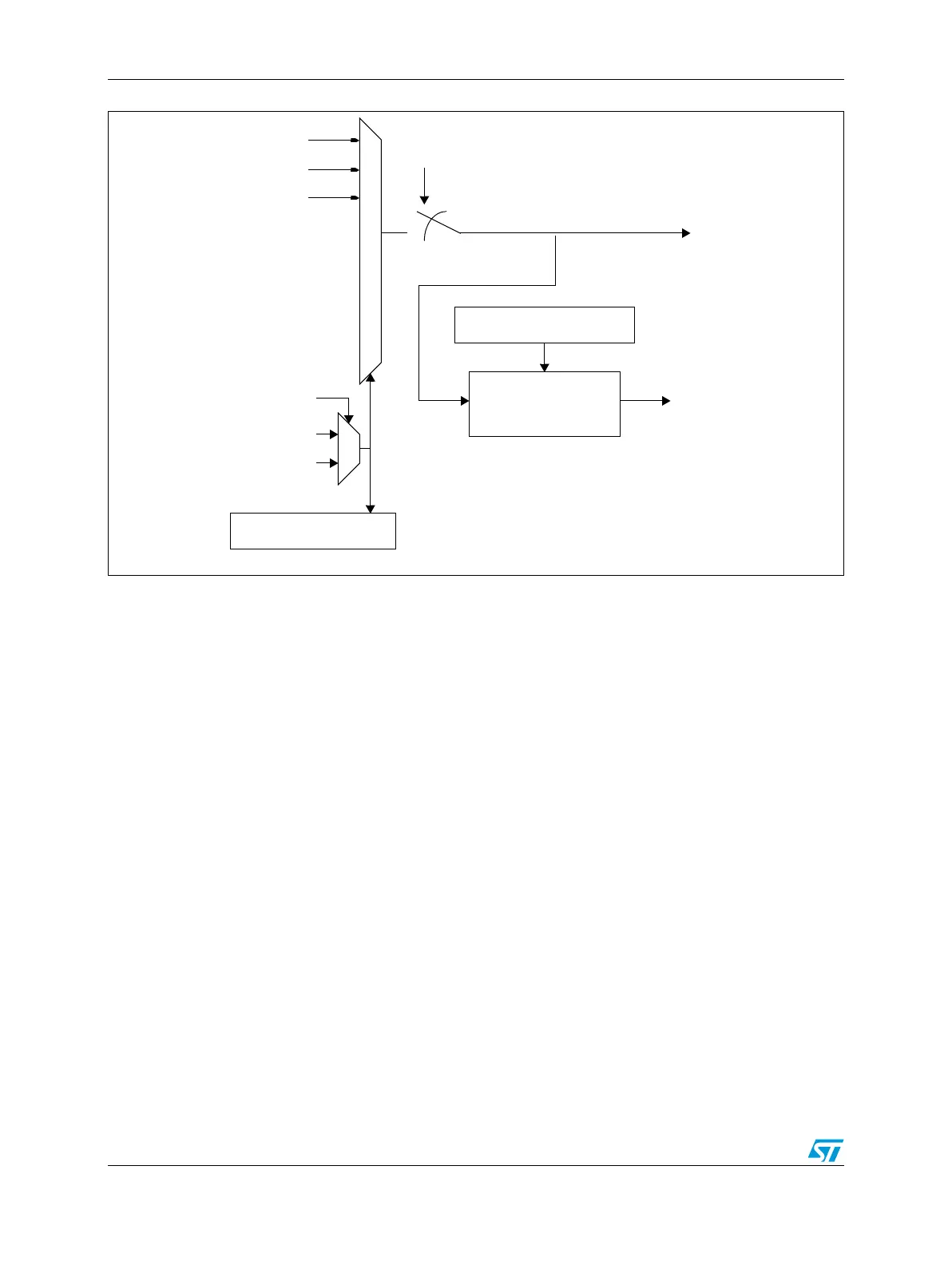
Figure 37. MC_CGM System Clock Generation Overview
5.7.1 System Clock Source Selection
During normal operation, the system clock selection is controlled
● on a SAFE mode or reset event, by the MC_RGM
● otherwise, by the MC_ME
5.7.2 System Clock Disable
During the TEST mode, the system clock can be disabled by the MC_ME.
5.7.3 System Clock Dividers
The MC_CGM generates the divided system clock 0 - controlled by the CGM_SC_DC0
register.
5.8 Auxiliary Clock Generation
Figure 38 shows the block diagram of the auxiliary clock generation logic. See
Section 5.5.5, “Auxiliary Clock 0 Select Control Register (CGM_AC0_SC), Section 5.5.7,
“Auxiliary Clock 1 Select Control Register (CGM_AC1_SC), and Section 5.5.9, “Auxiliary
Clock 2 Select Control Register (CGM_AC2_SC) for auxiliary clock selection control.
4 MHz crystal osc. 2
system PLL 4
system clock
’0’
CGM_SC_SS Register
MC_RGM SAFE mode request
ME_<current mode>
_MC.SYSCLK
CGM_SC_DC0 Register
clock divider
divided system clock 0
system clock is disabled if
ME_<current mode>_MC.SYSCLK = “1111”
“0000” 1
0
16 MHz int. RC osc. 0