RM0046 FlexPWM
Doc ID 16912 Rev 5 659/936
Value register 5 (VAL5)
The 16-bit signed value in this register defines the count value to set PWMB low
(Figure 334). This register is not byte accessible.
Note: The VAL5 register is buffered. The value written does not take effect until the LDOK bit is set
and the next PWM load cycle begins. VAL5 cannot be written when LDOK is set. Reading
VAL5 reads the value in a buffer and not necessarily the value the PWM generator is
currently using.
Output Control register (OCTRL)
Figure 344. Value register 5 (VAL5)
Address:
Base + 0x0012 (Submodule 0)
Base + 0x0062 (Submodule 1)
Base + 0x00B2 (Submodule 2)
Base + 0x0102 (Submodule 3) Access: User read/write
0123456789101112131415
R
VAL5
W
Reset0000000000000000
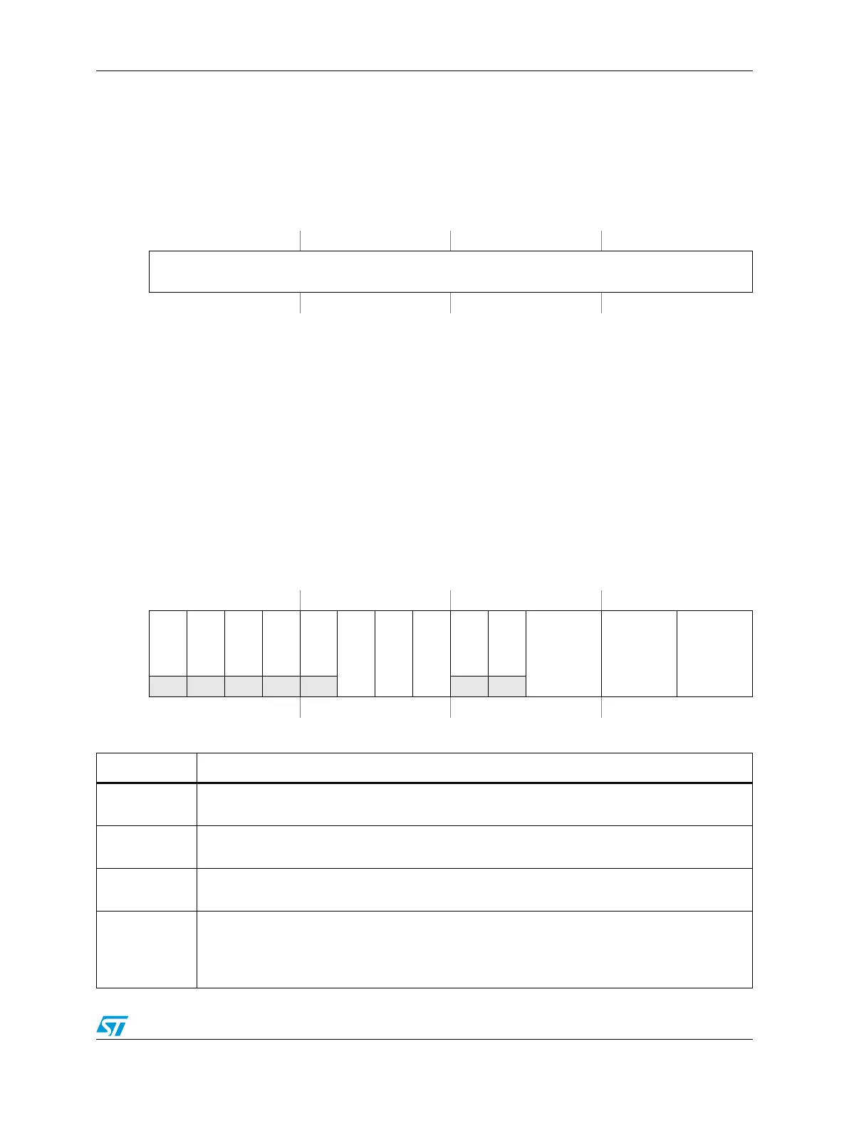
Figure 345. Output Control register (OCTRL)
Address:
Base + 0x0018 (Submodule 0)
Base + 0x0068 (Submodule 1)
Base + 0x00B8 (Submodule 2)
Base + 0x0108 (Submodule 3) Access: User read/write
0123456789101112131415
R
PWMA_IN
PWMB_IN
PWMX_IN
00
POLA
POLB
POLX
00
PWMAFS PWMBFS PWMXFS
W
Reset0000000000000000
Table 347. OCTRL field descriptions
Field Description
0
PWMA_IN
PWMA Input
This read only bit shows the logic value currently being driven into the PWMA input.
1
PWMB_IN
PWMB Input
This read only bit shows the logic value currently being driven into the PWMB input.
2
PWMX_IN
PWMX Input
This read only bit shows the logic value currently being driven into the PWMX input.
5
POLA
PWMA Output Polarity
This bit inverts the PWMA output polarity.
0 PWMA output not inverted. A high level on the PWMA pin represents the “on” or “active” state.
1 PWMA output inverted. A low level on the PWMA pin represents the “on” or “active” state.