RM0046 System Integration Unit Lite (SIUL)
Doc ID 16912 Rev 5 263/936
Parallel GPIO Pad Data Out register 0–3 (PGPDO[0:3])
These registers set or clear the respective pads of the device.
Note: The PGPDO registers access the same physical resource as the PDO and MPGPDO
address locations. Some examples of the mapping:
PPDO[0][0] = PDO[0]
PPDO[2][0] = PDO[32]
Parallel GPIO Pad Data In register 0–3 (PGPDI[0:3])
These registers hold the synchronized input value from the pads.
Table 104. GPDI[0_3:68_71] field descriptions
Field Description
PDI[x]
Pad Data In
This bit stores the value of the external GPIO pad associated with this register.
0: The value of the data in signal for the corresponding GPIO pad is logic low.
1: The value of the data in signal for the corresponding GPIO pad is logic high.
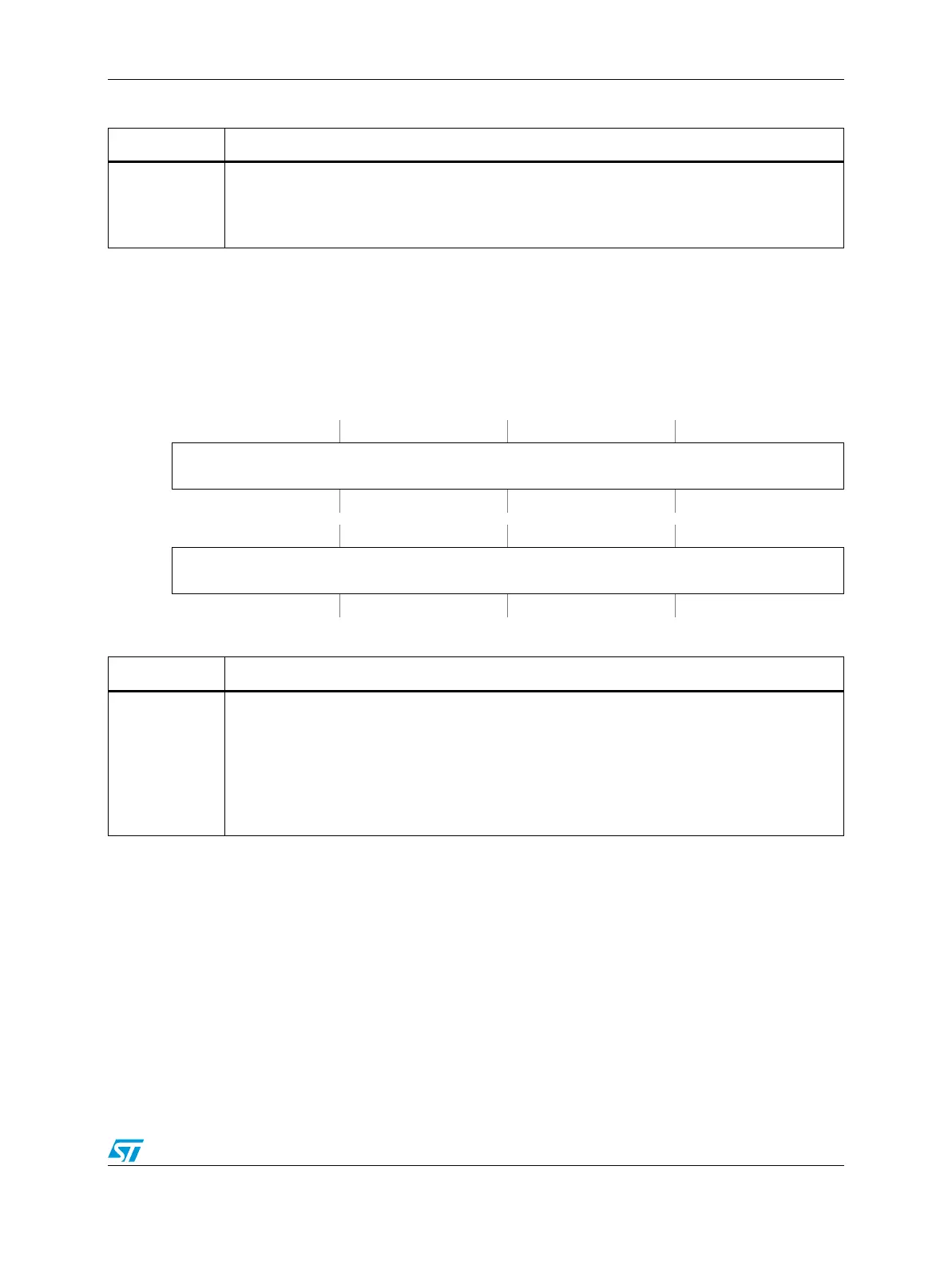
Figure 109. Parallel GPIO Pad Data Out register 0–3(PGPDO[0:3])
Address:
Base + 0x0C00 (PGPDO0)
Base + 0x0C04 (PGPDO1)
Base + 0x0C05 (PGPDO2)
Base + 0x0C0C (PGPDO3)
Access: User read/write
0123456789101112131415
R
PPDO[x][15:0]
W
Reset0000000000000000
16 17 18 19 20 21 22 23 24 25 26 27 28 29 30 31
R
PPDO[x + 1][15:0]
W
Reset0000000000000000
Table 105. PGPDO0_3 field descriptions
Field Description
PPDO[x]
Parallel Pad Data Out
Write or read the data register that stores the value to be driven on the pad in output mode.
Accesses to this register location are coherent with accesses to the bit-wise GPIO Pad Data
Output registers 0_3–68_71 (GPDO[0_3:68_71]).
The x and bit index define which PPDO register bit is equivalent to which PDO register bit
according to the following equation:
PPDO[x][y] = PDO[(x *16)+y]