Clock Generation Module (MC_CGM) RM0046
128/936 Doc ID 16912 Rev 5
5.5.6 Auxiliary Clock 0 Divider Configuration Register (CGM_AC0_DC0)
This register controls the auxiliary clock 0 divider.
5.5.7 Auxiliary Clock 1 Select Control Register (CGM_AC1_SC)
This register is used to select the current clock source for the following clocks:
● undivided: (unused)
● divided by auxiliary clock 1 divider 0: (unused)
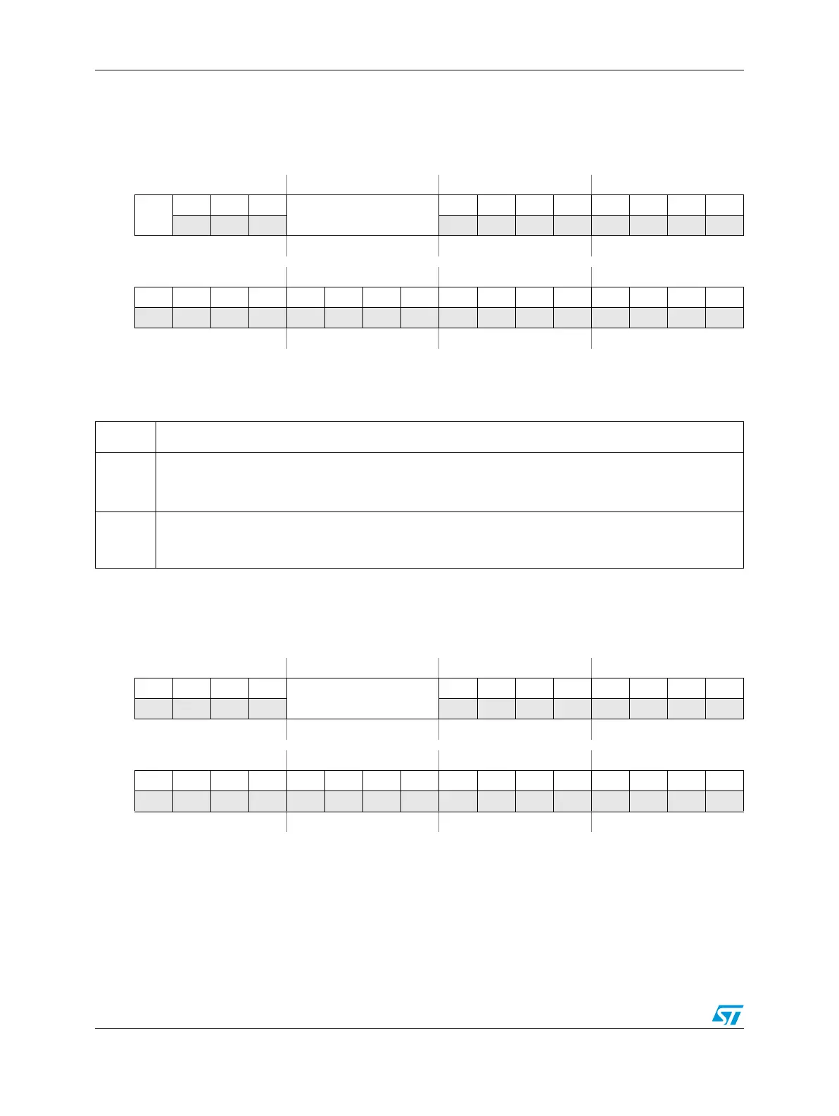
Figure 32. Auxiliary Clock 0 Divider Configuration Register (CGM_AC0_DC0)
Address 0xC3FE_0384 Access: User read, Supervisor read/write, Test read/write
0123456789101112131415
R
DE0
000
DIV0
00000000
W
Reset1000000000000000
16 17 18 19 20 21 22 23 24 25 26 27 28 29 30 31
R0000000000000000
W
Reset0000000000000000
Table 31. Auxiliary Clock 0 Divider Configuration Register (CGM_AC0_DC0) Field Descriptions
Field Description
DE0
Divider 0 Enable
0 Disable auxiliary clock 0 divider 0
1 Enable auxiliary clock 0 divider 0
DIV0
Divider 0 Division Value — The resultant (unused) will have a period DIV0 + 1 times that of auxiliary
clock 0. If the DE0 is set to 0 (Divider 0 is disabled), any write access to the DIV0 field is ignored and the
(unused) remains disabled.
Figure 33. Auxiliary Clock 1 Select Control Register (CGM_AC1_SC)
Address 0xC3FE_0388 Access: User read, Supervisor read/write, Test read/write
0123456789101112131415
R0000
SELCTL
00000000
W
Reset0000000000000000
16 17 18 19 20 21 22 23 24 25 26 27 28 29 30 31
R0000000000000000
W
Reset0000000000000000