IEEE 1149.1 Test Access Port Controller (JTAGC) RM0046
852/936 Doc ID 16912 Rev 5
controlling access to a resource, as well as controlling single-step operation and exit from
OnCE mode.
Although the OCMD is updated during the update-IR TAP controller state, the corresponding
resource is accessed in the DR scan sequence of the TAP controller, and as such, the
update-DR state must be transitioned through in order for an access to occur. In addition,
the update-DR state must also be transitioned through in order for the single-step and/or exit
functionality to be performed, even though the command appears to have no data resource
requirement associated with it.
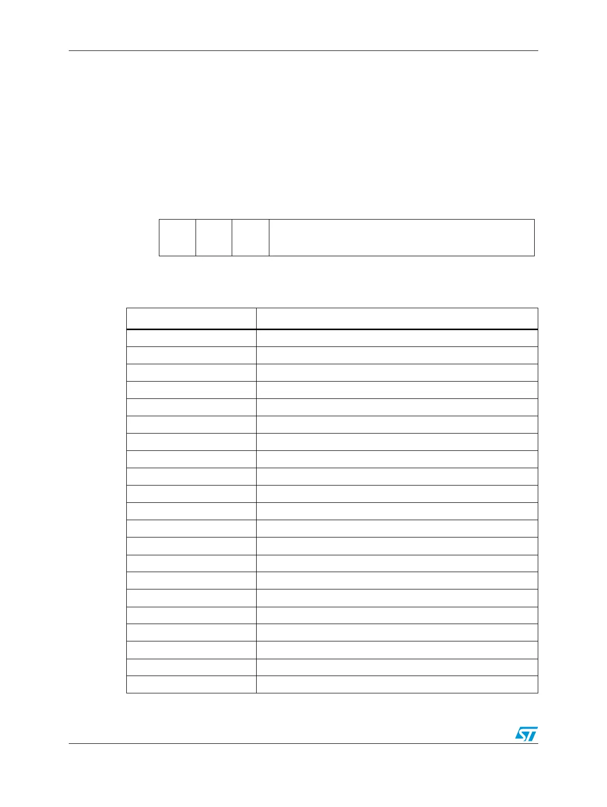
Figure 503. OnCE Command register (OCMD)
012 3 456789
R
R/W GO EX RS[0:6]
W
Reset000 0 011011
Table 457. e200z0 OnCE register addressing
RS[0:6] Register selected
000 0000 000 0001 Reserved
000 0010 JTAG ID (read-only)
000 0011 – 000 1111 Reserved
001 0000 CPU Scan Register (CPUSCR)
001 0001 No Register Selected (Bypass)
001 0010 OnCE Control Register (OCR)
001 0011 – 001 1111 Reserved
010 0000 Instruction Address Compare 1 (IAC1)
010 0001 Instruction Address Compare 2 (IAC2)
010 0010 Instruction Address Compare 3 (IAC3)
010 0011 Instruction Address Compare 4 (IAC4)
010 0100 Data Address Compare 1 (DAC1)
010 0101 Data Address Compare 2 (DAC2)
010 0110 Data Value Compare 1 (DVC1)
010 0111 Data Value Compare 2 (DVC2)
010 1000 – 010 1111 Reserved
011 0000 Debug Status Register (DBSR)
011 0001 Debug Control Register 0 (DBCR0)
011 0010 Debug Control Register 1 (DBCR1)
011 0011 Debug Control Register 2 (DBCR2)
011 0100 – 101 1111 Reserved (do not access)

 Loading...