RM0046 Nexus Development Interface (NDI)
Doc ID 16912 Rev 5 891/936
command (See Section , “e200z0h OnCE Command Register (OCMD)). The CPU will then
temporarily exit the debug state (but not
the debug session) to execute the instruction, and
will then return to the debug state (again indicated via the OnCE Status Register (OSR)).
The debug session remains in force until the final OnCE go+exit command is executed, at
which time the CPU will return to the previous state it was in (unless a new debug request is
pending). A scan into the CPUSCR is required
prior to executing each go+exit or go+noexit
OnCE command.
36.12.2 JTAG/OnCE Pins
The JTAG/OnCE pin interface is used to transfer OnCE instructions and data to the OnCE
control block. Depending on the particular resource being accessed, the CPU may need to
be placed in the Debug mode. For resources outside of the CPU block and contained in the
OnCE block, the processor is not disturbed, and may continue execution. If a processor
resource is required, an internal debug request (dbg_dbgrq) may be asserted to the CPU
by the OnCE controller, and causes the CPU to finish the current instruction being executed,
save the instruction pipeline information, enter Debug Mode, and wait for further commands.
Asserting dbg_dbgrq will cause the chip to exit the low power mode enabled by the setting
of MSR
WE
, as well as temporarily exiting the waiting, stopped or halted power management
states.
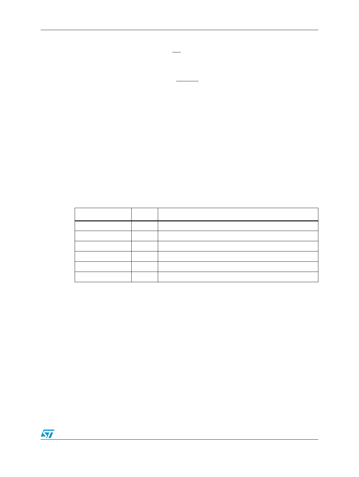
Table 466 details the primary JTAG/OnCE interface signals.
36.12.3 OnCE Internal Interface Signals
The following paragraphs describe the OnCE interface signals to other internal blocks
associated with the OnCE controller.
CPU Debug Request (dbg_dbgrq)
The dbg_dbgrq signal is asserted by the OnCE control logic to request the CPU to enter
the debug state. It may be asserted for a number of different conditions, and causes the
CPU to finish the current instruction being executed, save the instruction pipeline
information, enter the debug mode, and wait for further commands.
CPU Debug Acknowledge (cpu_dbgack)
The cpu_dbgack signal is asserted by the CPU upon entering the debug state. This signal
is used as part of the handshake mechanism between the OnCE control logic and the rest
Table 466. JTAG/OnCE Primary Interface Signals
Signal Name Type Description
j_trst_b I JTAG test reset
j_tclk I JTAG test clock
j_tms I JTAG test mode select
j_tdi I JTAG test data input
j_tdo O Test data out to master controller or pad
j_tdo_en
(1)
1. j_tdo_en is asserted when the TAP controller is in the shift_DR or shift_IR state.
O Enables TDO output buffer