RM0046 Clock Generation Module (MC_CGM)
Doc ID 16912 Rev 5 129/936
5.5.8 Auxiliary Clock 1 Divider Configuration Register (CGM_AC1_DC0)
This register controls the auxiliary clock 1 divider.
Table 32. Auxiliary Clock 1 Select Control Register (CGM_AC1_SC) Field Descriptions
Field Description
SELCTL
Auxiliary Clock 1 Source Selection Control — This value selects the current source for auxiliary clock
1.
0000 (no clock)
0001 reserved
0010 reserved
0011 reserved
0100 reserved
0101 reserved
0110 reserved
0111 reserved
1000 reserved
1001 reserved
1010 reserved
1011 reserved
1100 reserved
1101 reserved
1110 reserved
1111 reserved
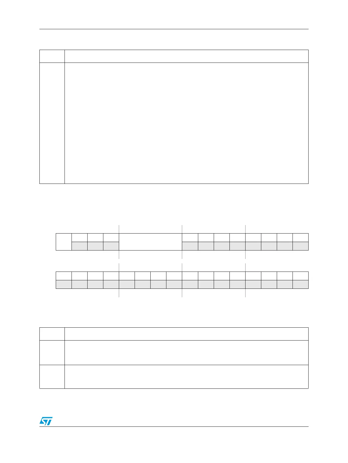
Figure 34. Auxiliary Clock 1 Divider Configuration Register (CGM_AC1_DC0)
Address 0xC3FE_038C Access: User read, Supervisor read/write, Test read/write
0123456789101112131415
R
DE0
000
DIV0
00000000
W
Reset1000000000000000
16 17 18 19 20 21 22 23 24 25 26 27 28 29 30 31
R0000000000000000
W
Reset0000000000000000
Table 33. Auxiliary Clock 1 Divider Configuration Register (CGM_AC1_DC0) Field Descriptions
Field Description
DE0
Divider 0 Enable
0 Disable auxiliary clock 1 divider 0
1 Enable auxiliary clock 1 divider 0
DIV0
Divider 0 Division Value — The resultant (unused) will have a period DIV0 + 1 times that of auxiliary
clock 1. If the DE0 is set to 0 (Divider 0 is disabled), any write access to the DIV0 field is ignored and the
(unused) remains disabled.