Flash Memory RM0046
314/936 Doc ID 16912 Rev 5
system memory map defines one code Flash array and one data Flash array. See
Table 137.
Caution:
Software executing from flash memory must not write to registers that control flash behavior
(such as wait state settings or prefetch enable/disable). Doing so can cause data corruption.
On this chip, these registers include PFCR0 and PFAPR.
Note: Flash memory configuration registers should be written only with 32-bit write operations to
avoid any issues associated with register incoherency caused by bit fields spanning smaller
size (8-, 16-bit) boundaries.
For additional information on the address-based read access timing for emulation of other
memory types, see Section 17.2.17, “Wait state emulation.
Next, consider the memory map associated with the control and configuration registers.
There are multiple registers that control operation of the platform Flash controller. Note the
first two Flash array registers (PFCR0, PFCR1) are reset to a device-defined value, while
the remaining register (PFAPR) is loaded at reset from specific locations in the array’s
shadow region.
Regardless of the number of populated banks or the number of Flash arrays included in a
given bank, the configuration of the platform Flash controller is wholly specified by the
platform Flash controller control registers associated with code Flash array0. The code
array0 register settings define the operating behavior of both Flash banks. It is
recommended to set the platform Flash controller control registers for both arrays to the
array0 values.
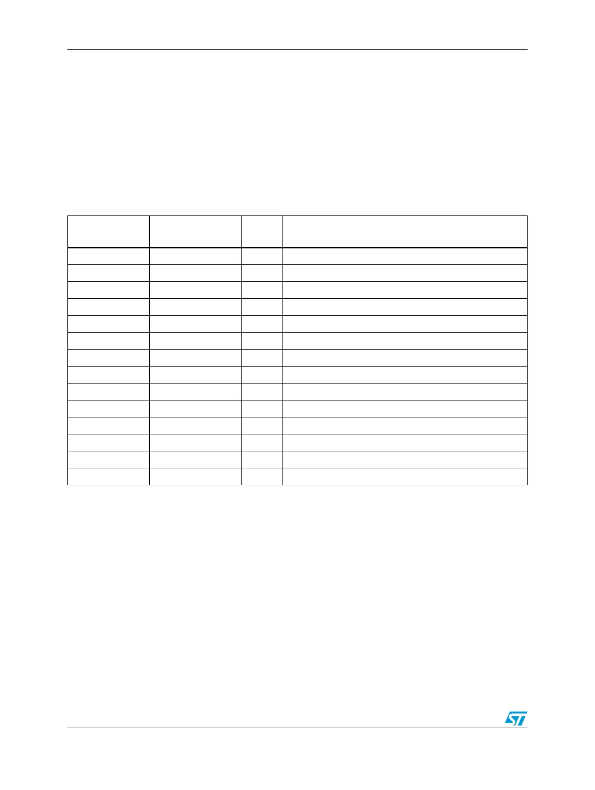
Table 137. Flash-related regions in the system memory map
Start address End address
Size
(KB)
Region
0x0000_0000 0x0007_FFFF 512 Code Flash array 0
0x0008_0000 0x001F_FFFF 1536 Reserved
0x0020_0000 0x0020_3FFF 16 Code Flash array 0: shadow sector
0x0020_4000 0x003F_FFFF 2032 Reserved
0x0040_0000 0x0040_3FFF 16 Code Flash array 0: test sector
0x0040_4000 0x007F_FFFF 4080 Reserved
0x0080_0000 0x0080_FFFF 64 Data Flash array 0
0x0081_0000 0x00C0_1FFF 4040 Reserved
0x00C0_2000 0x00C0_3FFF 8 Data Flash array 0: test sector
0x00C0_4000 0x00FF_FFFF 4080 Reserved
0x0100_0000 0x1FFF_FFFF 507904 Emulation Mapping
0xFFE8_8000 0xFFE8_BFFF 16 Code Flash array 0 configuration
(1)
0xFFE8_C000 0xFFE8_FFFF 16 Data Flash array 0 configuration
(1)
0xFFEB_0000 0xFFEB_BFFF 48 Reserved
1. This region is also aliased to address 0xC3F8_nnnn.