RM0046 Flash Memory
Doc ID 16912 Rev 5 363/936
User Test 2 register (UT2)
The User Test 2 register allows to enable the checks on the ECC logic related to the 32 MSB
of the Double Word.
The User Test 2 register is not accessible whenever MCR[DONE] or UT0[AID] are low.
Reads return indeterminate data. Writes have no effect.
Note: This register is not implemented on the data Flash block.
User Multiple Input Signature Register 0 (UMISR0)
The Multiple Input Signature Register 0 (UMISR0) provides a mean to evaluate the array
integrity. UMISR0 represents the bits 31:0 of the whole 144-bit word (2 double words
including ECC).
UMISR0 is not accessible whenever MCR[DONE] or UT0[AID] are low. Reads return
indeterminate data. Writes have no effect.
Table 160. UT1 field descriptions
Field Description
DAI[31:0]
0:31
Data Array Input 31–0
These bits represent the input of the even word of ECC logic used in the ECC Logic Check.
The DAI[31:0] bits correspond to the 32 array bits representing Word 0 within the double word.
0 The array bit is forced at 0.
1 The array bit is forced at 1.
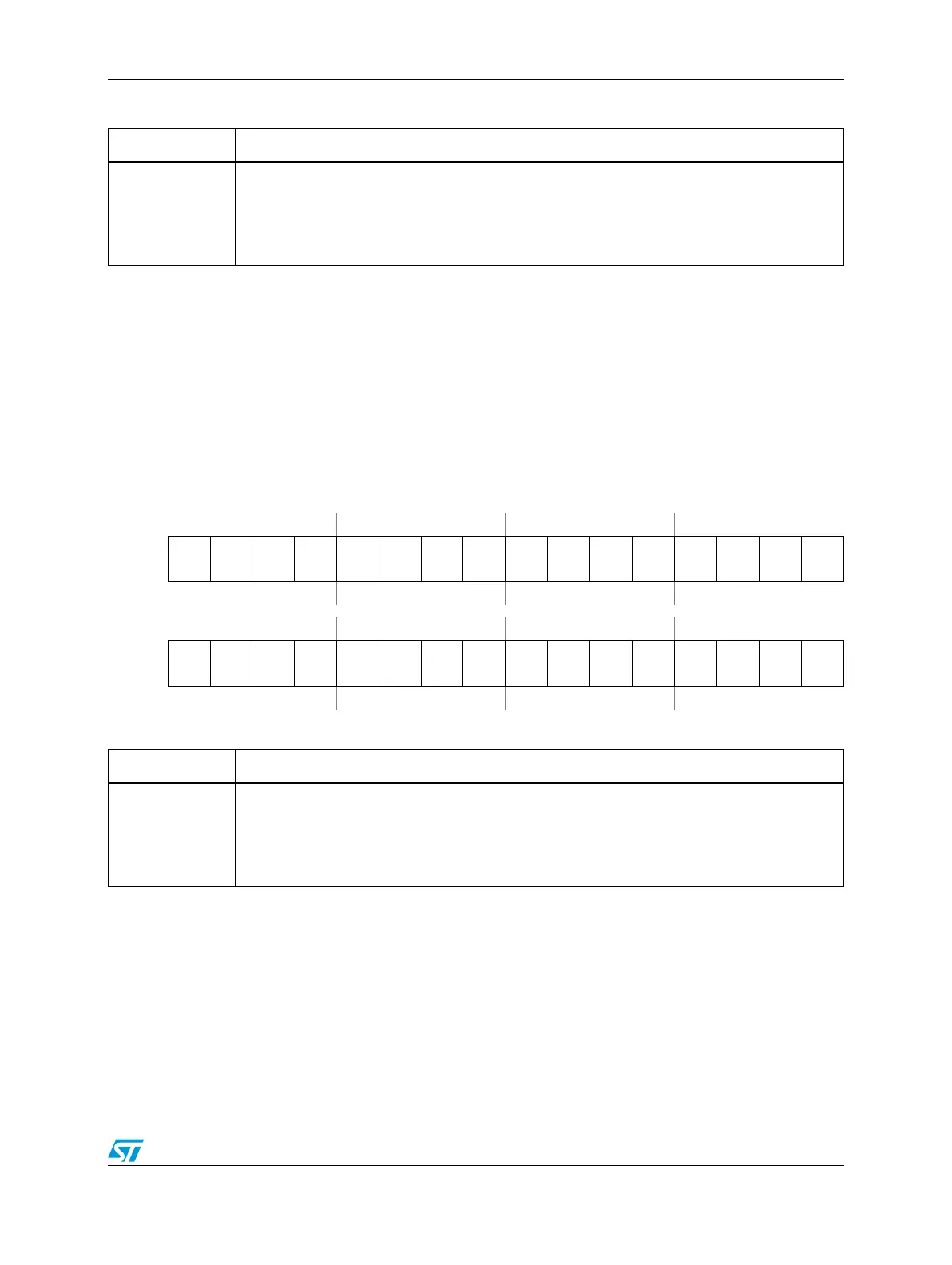
Figure 165. User Test 2 register (UT2)
Address:
Base + 0x0044 Access: User read/write
0123456789101112131415
R
DAI
63
DAI
62
DAI
61
DAI
60
DAI
59
DAI
58
DAI
57
DAI
56
DAI
55
DAI
54
DAI
53
DAI
52
DAI
51
DAI
50
DAI
49
DAI
48
W
Reset0000000000000000
16 17 18 19 20 21 22 23 24 25 26 27 28 29 30 31
R
DAI
47
DAI
46
DAI
45
DAI
44
DAI
43
DAI
42
DAI
41
DAI
40
DAI
39
DAI
38
DAI
37
DAI
36
DAI
35
DAI
34
DAI
33
DAI
32
W
Reset0000000000000000
Table 161. UT2 field descriptions
Field Description
DAI[63:32]
0:31
Data Array Input [63:32]
These bits represent the input of the odd word of ECC logic used in the ECC Logic Check. The
DAI[63:32] bits correspond to the 32 array bits representing Word 1 within the double word.
0 The array bit is forced at 0.
1 The array bit is forced at 1.