RM0046 IEEE 1149.1 Test Access Port Controller (JTAGC)
Doc ID 16912 Rev 5 843/936
Bypass mode
When no test operation is required, the BYPASS instruction can be loaded to place the
JTAGC into bypass mode. While in bypass mode, the single-bit bypass shift register
provides a minimum-length serial path to shift data between TDI and TDO.
TAP sharing mode
There are four selectable auxiliary TAP controllers that share the TAP with the JTAGC.
Selectable TAP controllers include the Nexus port controller (NPC), e200 OnCE, and eDMA
Nexus. The instructions required to grant ownership of the TAP to the auxiliary TAP
controllers are ACCESS_AUX_TAP_ONCE and ACCESS_AUX_TAP_NPC. Instruction
opcodes for each instruction are shown in Table 4 5 6.
When the access instruction for an auxiliary TAP is loaded, control of the JTAG pins is
transferred to the selected TAP controller. Any data input via TDI and TMS is passed to the
selected TAP controller, and any TDO output from the selected TAP controller is sent back to
the JTAGC to be output on the pins. The JTAGC regains control of the JTAG port during the
UPDATE-DR state if the PAUSE-DR state was entered. Auxiliary TAP controllers are held in
RUN-TEST/IDLE while they are inactive.
For more information on the TAP controllers refer to 36, “Nexus Development Interface
(NDI).
35.6 External signal description
The JTAGC consists of four signals that connect to off-chip development tools and allow
access to test support functions. The JTAGC signals are outlined in Ta bl e 45 4 .
35.7 Memory map and registers description
This section provides a detailed description of the JTAGC registers accessible through the
TAP interface, including data registers and the instruction register. Individual bit-level
descriptions and reset states of each register are included. These registers are not memory-
mapped and can only be accessed through the TAP.
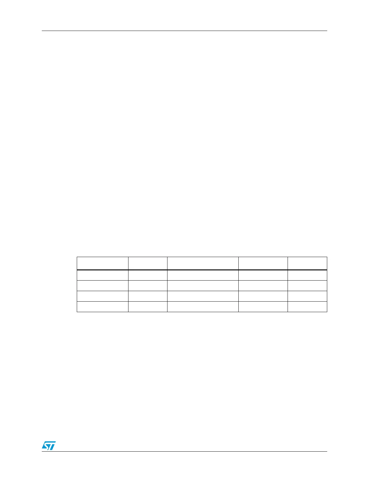
Table 454. JTAG signal properties
(1)
1. Test clock frequency must always be less than one fourth of system clock frequency.
Name I/O Function Reset state Pull
(2)
2. The pull is not implemented in this module. Pullup/down devices are implemented in the pads.
TCK I Test clock — Down
TDI I Test data in — Up
TDO O Test data out High Z
(3)
3. TDO output buffer enable is negated when JTAGC is not in the Shift-IR or Shift-DR states. A weak
pulldown can be implemented on TDO.
Down
(3)
TMS I Test mode select — Up